MPC5746R Hardware Design Guide, Rev. 1
Example Communication Peripheral connections
NXP Semiconductors42
Control
1kŸ
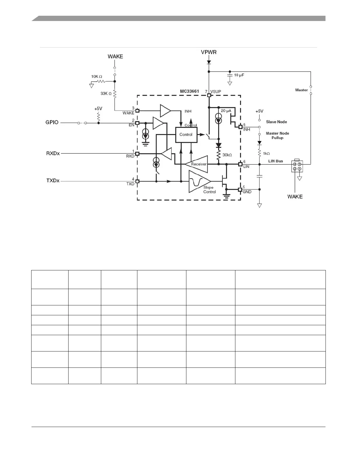
Figure 28. Typical LIN connections
Table 20 below shows the pins of the MC33661 and their typical connections to a MCU.
Table 20. MC33661 Pin Definitions and Example System Connections
Pin Number Pin Name Pin Direction Full Pin Name
MCU or System
Connection
Description
1 RXD Output
Receive Data
Output
MCU LIN RXD
LIN receive data output to the MCU.
2 EN Input Enable Control MCU GPIO Enable operation of the device.
3 Wake Input Wake Input LIN Bus Wake
1
Enables the device out of sleep mode.
4 TXD Input Transmit Data Input MCU LIN TXD LIN transmit data input from the MCU.
5 GND Input Ground
System Ground
Reference
Device ground reference.
6 LIN Input/Output LIN Bus LIN Bus
Bi-directional pin that represents the
single-wire transmit and receive.
7 VSUP Input Power Supply
Protected Battery
Voltage
Device power supply, typically
connected to a nominal 12 V supply.

 Loading...


