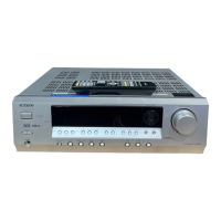
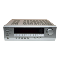
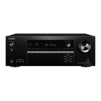
TX-SR303 Silver model
Ref. No. 3862
042005
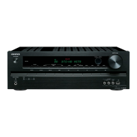
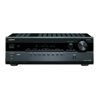
AV RECEIVER
120V AC, 60HzMDD
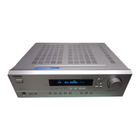
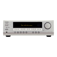
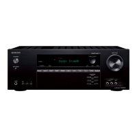
TX-SR303E Silver model
230-240V AC, 50HzMPP
MODEL TX-SR303
MODEL TX-SR303E
RC-605S
TONE
+
STEREO
LISTENING MODE
DISPLAY
DIGITAL INPUT
DIMMER MEMORY
TUNING MODE
RETURN
TUNING / PRESET
ENTER
SETUP
STANDBY
STANDBY/ON
CLEAR
PHONES
MULTl CH DVD VIDEO 1/VCR VIDEO 2 VIDEO 3 TAPE TUNER CD
MASTER VOLUME
A SPEAKERS B
MUTING
MENUTOP MENU
SP A
/
B
SETUPRETURN
RANDOM
SUBTITLE
PLAY MODE
AUDIO REPEAT
RC
-
605S
--
/
---
TAPE /AM P
ON STANDBY
DIMMER SLEEP
INPUT SELECTOR
REMOTE MODE
V
1
V
2
V
3
C
DTAPE TUNER
DVD
MULTI CH
LISTENING MODE
DISPLAY
TEST
TONE
CH SEL
SURROUND
STEREO
CINE FLTR
LEVEL
+
LEVEL
-
L NIGHT
VOL
CDR
MD
DVD
RECEIVER
C
D
+
10
0
CLR
123
456
789
ENTER
CH
DISC
SAFETY-RELATED COMPONENT
WARNING!!
COMPONENTS IDENTIFIED BY MARK ON THE
SCHEMATIC DIAGRAM AND IN THE PARTS LIST ARE
CRITICAL FOR RISK OF FIRE AND ELECTRIC SHOCK.
REPLACE THESE COMPONENTS WITH ONKYO
PARTS WHOSE PART NUMBERS APPEAR AS SHOWN
IN THIS MANUAL.
MAKE LEAKAGE-CURRENT OR RESISTANCE
MEASUREMENTS TO DETERMINE THAT EXPOSED
PARTS ARE ACCEPTABLY INSULATED FROM THE
SUPPLY CIRCUIT BEFORE RETURNING THE
APPLIANCE TO THE CUSTOMER.