1 Safety Precaution 4
1.1. General guidelines
4
1.2. Caution for fuse replacement
4
2 Warning
5
2.1. Prevention of Electrostatic Discharge (ESD) to
Electrostatic Sensitive (ES) Devices 5
2.2. Precaution of Laser Diode
6
2.3. Service caution based on legal restrictions
7
3 Service Navigation
8
3.1. Service Information
8
3.2. Caution for DivX
8
4 Specifications
9
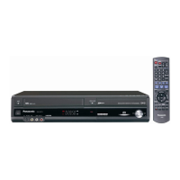
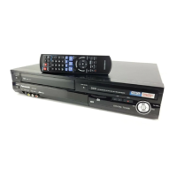
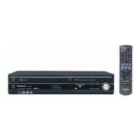
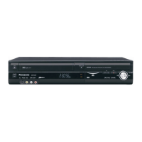
5 Location of Controls and Components
10
5.1. Each Buttons
10
6 Operation Instructions
12
6.1. (DVD) Taking out the Disc from RAM-Drive Unit when the
Disc cannot be ejected by OPEN/CLOSE button
12
6.2. (VHS) Removing Cassette Tape manually
14
7 Service Mode
16
7.1. (DVD) Self-Diagnosis and Special Mode Setting
16
7.2. (VHS) Self-Diagnosis and Special Mode Setting
26
8 Service Fixture & Tools
32
9 Assembling and Disassembling Instructions
33
9.1. Disassembly Flow Chart
33
9.2. P.C.B. Positions
34
9.3. Caution with inserting cassette tape when disassembling
the unit 35
9.4. Top cover
36
9.5. Front Panel
36
9.6. Front (L) P.C.B. & Front (R) P.C.B.
37
9.7. DVD drive
39
9.8. SD/DV Jack P.C.B.
39
9.9. Rear Panel, Fan Motor
40
9.10. Digital P.C.B.
40
9.11. VHS Mechanism Unit
41
9.12. Main P.C.B.
42
9.13. Digital I/F P.C.B.
42
10 Measurements and Adjustments
43
10.1. Service Positions
43
10.2. Caution for Replacing Parts
47
10.3. Standard Inspection Specifications after Making Repairs
50
11 Block Diagram 53
11.1. Power Supply Block Diagram 53
11.2. Main P.C.B. Regulator Block Diagram
54
11.3. Analog Video Block Diagram 55
11.4. Analog Audio Block Diagram 57
11.5. Analog Timer Block Diagram
58
11.6. System Control & Servo Block Diagram
59
12 Schematic Diagram
61
12.1. Interconnection Schematic Diagram
61
12.2. Power Supply Section (Power & Digital I/F P.C.B.(1/3))
Schematic Diagram (P) 63
12.3. Digital I/F (1/4) Section (Power & Digital I/F P.C.B.(2/3))
Schematic Diagram (IF)
65
12.4. Digital I/F (2/4) Section (Power & Digital I/F P.C.B.(2/3))
Schematic Diagram (IF) 66
12.5. Digital I/F (3/4) Section (Power & Digital I/F P.C.B.(2/3))
Schematic Diagram (IF)
67
12.6. Digital I/F (4/4) Section (Power & Digital I/F P.C.B.(2/3))
Schematic Diagram (IF) 68
12.7. Tuner Section (Power & Digital I/F P.C.B.(3/3)) Schematic
Diagram (IF)
69
12.8. Video Section (Main P.C.B.(1/4)) Schematic Diagram (V)
70
12.9. VHS Audio Section (Main P.C.B.(2/4)) Schematic Diagram
(A) 71
12.10. Syscon/Servo/Timer (1/4) Section (Main P.C.B.(3/4))
Schematic Diagram (S)
72
12.11. Syscon/Servo/Timer (2/4) Section (Main P.C.B.(3/4))
Schematic Diagram (S) 73
12.12. Syscon/Servo/Timer (3/4) Section (Main P.C.B.(3/4))
Schematic Diagram (S)
74
12.13. Syscon/Servo/Timer (4/4) Section (Main P.C.B.(3/4))
Schematic Diagram (S) 75
12.14. I/O Section (1/4) (Main P.C.B.(4/4)) Schematic Diagram (I)
77
12.15. I/O Section (2/4) (Main P.C.B.(4/4)) Schematic Diagram (I)
78
12.16. I/O Section (3/4) (Main P.C.B.(4/4)) Schematic Diagram (I)
79
12.17. I/O Section (4/4) (Main P.C.B.(4/4)) Schematic Diagram (I)
80
12.18. DV Jack/SD Card Schematic Diagram
82
12.19. Front (L) Schematic Diagram
83
12.20. Front (R) Schematic Diagram
83
13 Printed Circuit Board
85
13.1. Power & Digital I/F P.C.B.
85
13.2. Main P.C.B. 90
13.3. DV Jack/SD Card P.C.B. 95
13.4. Front (L) P.C.B., Front (R) P.C.B.
96
14 Appendix for Schematic Diagram 97
14.1. Voltage and Waveform Chart 97
CONTENTS
Page Page
2
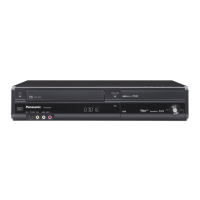
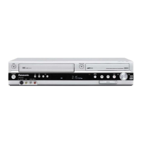
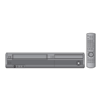
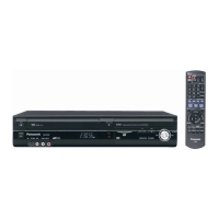
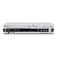
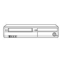
DMR-EZ47VP / DMR-EZ475VP
 Loading...