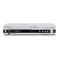
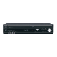
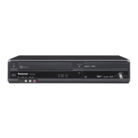
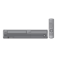
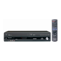
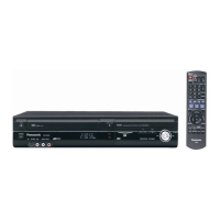
Do you have a question about the Panasonic DMR-EZ45VEB and is the answer not in the manual?
General safety guidelines and procedures for leakage current checks.
Precautions to prevent component damage from ESD.
Safety measures for handling laser diodes.
Cautions regarding lead-free solder use and environmental compliance.
Details service manual scope and excluded information.
Forcible ejection of a DVD disc when standard methods fail.
Methods for removing a VHS cassette tape manually.
Manual VHS cassette removal after mechanism disassembly.
Details DVD self-diagnosis error codes and functions.
Setting various special modes for DVD servicing.
Lists and describes specific DVD service modes.
Covers VHS self-diagnosis, special modes, and service modes.
Details VHS self-diagnosis error code memory and history.
Provides a flowchart for unit disassembly.
Diagrams showing the location of various PCBs within the unit.
Caution regarding cassette tape handling during disassembly.
Step-by-step procedure for removing the top case.
Step-by-step procedure for removing the front panel.
Procedure for removing Front Jack and FL Drive PCBs.
Procedure for removing the rear panel and fan motor.
Procedure for removing the VCR mechanism unit.
Important caution for reattaching the VCR mechanism.
Procedure for removing the main PCB.
Procedure for removing the tuner module.
Procedure for removing the DVD-RAM Drive/Digital PCB module.
Procedure for removing the SD/DV Input PCB.
Procedure for removing the Power & Digital I/F PCB.
Procedure for removing the back end PCB.
Procedure for removing the HDMI PCB.
Specifies positions for PCB measurements and repairs.
Steps for checking and repairing the Power & Digital I/F PCB.
Steps for checking and repairing the main PCB.
Procedure for checking and replacing the DVD-RAM Drive/Digital PCB module.
Cautions and notices related to replacing internal parts.
Procedure for automatic adjustment of the PG shifter.
Procedure for adjusting X-Value and Linearity (P2/P3).
Procedure for adjusting the LINEARITY for flat envelope.
Comprehensive list of abbreviations used in the manual.
Block diagram of the power supply circuit.
Block diagram of system control, servo, and timer functions.
Block diagram illustrating the audio signal path.
Block diagram illustrating the video signal path.
Block diagram of the digital interface PCB.
Block diagram of the HDMI interface.
Shows interconnections between major assemblies and PCBs.
Schematic diagram of the power supply circuit.
Schematic diagram of the digital interface PCB.
Schematic diagram for I/O and tuner sections.
Schematic of system control, servo, and timer main unit.
Schematic diagram of the video processing circuitry.
Schematic diagram for the NICAM audio processing.
Schematic diagram of the front panel jack connections.
Schematic diagram of the FL display drive circuit.
Schematic diagram of the SD/DV Input PCB.
Schematic diagram of the HDMI interface PCB.
Component layout diagram for the Power & Digital I/F PCB.
Solder side layout diagram for the Power & Digital I/F PCB.
Component layout diagram for the Main PCB.
Solder side layout diagram for the Main PCB.
Component and solder side layout for the Front Jack PCB.
Component and solder side layout for the FL Drive PCB.
Component and solder side layout for the SD/DV Input PCB.
Component and solder side layout for the HDMI PCB.
Charts of standard voltage and waveform values for service.
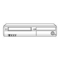
Exploded view of the mechanism and casing components.
Exploded view of the front panel assembly and its parts.
Exploded view of the VHS mechanism components.
Diagram of the product's packing and included accessories.
List of replacement casing and PCB parts with part numbers.
List of replacement parts for the VHS mechanism.
List of replacement packing and accessory parts.
List of replacement electrical components (capacitors, resistors, etc.).
List of service fixtures and tools with part numbers.
| Type | DVD Recorder |
|---|---|
| Weight | 3.5 kg |
| Progressive Scan | Yes |
| Hard Disk Capacity | 160 GB |
| Recording Format | DVD-RAM, DVD-R, DVD-RW |
| Video Formats Supported | MPEG-2 |
| Audio Formats Supported | Dolby Digital |
| Connections | Composite video output, S-Video output |
| Dimensions (W x H x D) | 430 x 59 x 286 mm |
| Video D/A Converter | 10-bit |
| Audio D/A Converter | 24-bit |
| Playback Format | DVD-Video, DVD-RAM, DVD-R, DVD-RW, CD, CD-R, CD-RW |
| Video Recording Format | MPEG2 |
| Audio Recording Format | Dolby Digital |
| Output Resolution | 1080p |