|61 |
TROUBLESHOOTING GUIDE
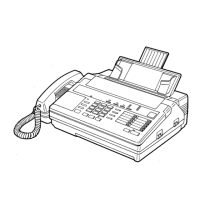
KX-F680BX/KX-F2681BX
CH1 5V/div
CH2 5V/div
CH3 5V/div
CH4 5V/div
W1 500ns/div
Length 100
W2 5µs/div
Length 1k
Sampling
Normal
20Msps
Marker 1
T -13.75µs
V 5.0 V
Marker 2
T 7.50µs
V 0.2 V
T 21.25µs
1/ T
47.06k Hz
V -4.8 V
Time
Time Base Roll
Off
Time Base
External
Internal
Internal
-40.0V
-17.75µs -12.75µs
Time/div
10.0V
H1 W1
A0
D0
ROMCS
RD
OK
W1 500ns
W2 5µs
Position
W1 -17.75µs
W2 -24.80µs
CH1 5V/div
CH2 5V/div
CH3 5V/div
CH4 5V/div
W1 500ns/div
Length 100
W2 5µs/div
Length 1k
Sampling
Normal
20Msps
Marker 1
T -13.75µs
V 5.0 V
Marker 2
T 7.50µs
V 0.2 V
T 21.25µs
1/ T
47.06kHz
V -4.8 V
W1 500ns
W2 5µs
Position
W1 7.25µs
W2 25.00µs
Time
Time Base Roll
Off
Time Base
External
Internal
Internal
-40.0V
7.25µs 12.25µs
Time/div
10.0V
H1 W1
A0
D0
ROMCS
RD
OK
Let's observe the wave form to fix the defective IC.
Please observe A0, D0, ROMCE, RD by using digital oscilloscope.
Below graph show you the wave form that is observed when unit
(board) is working correctly. Both graph are good wave. Wave
form is rapidly changing by one (like below graph). Because many
kind of data or program are rapidly executed,
so you can see some kind of wave forms that is seem to below
graph.
A0 : pin 132 of ASIC (IC1)
D0 : pin 131 of ASIC (IC1)
ROMCE : pin 22 of ROM (IC2)
RD : pin 24 of ROM (IC2)
SRAMCS: : pin 20 of SRAM(IC3)
MDMCS : pin 52 of MODEM(IC5)
name
location

 Loading...