CIRCUIT OPERATIONS
- 115 -
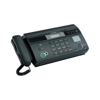
KX-FT21LA
2.ROM (IC2)
This 128 KB ROM (OTPROM or MASKROM) has 32 KB of common area and bank area (BK4~BK15).
The capacity of each bank is 8 KB.
The addresses of the common area are from 0000H to 7FFFH, and addresses 8000H to 9FFFH are for the bank
area.
3. RAM (IC3)
This 32 KB RAM has 8 KB of common area and bank area (BK0, BK1).
The capacity of each bank is 12 KB.
The addresses of the common area are from D000H to EFFFH, and addresses A000H to CFFFH are for the
bank area.
162
STB4 MULT3/5
NO OPEN O
Not used
163
THDAT MULT3/5
NO TH DATA O
Thermal data
164
VSS
DG
Ground
165
MULT3/5
- +5V
Pow er supply for THCLK, DAT, LAT, STB
166
THCLK MULT3/5
NO TH CLK O
Thermal head clock
167
THLAT MULT3/5
NO TH LAT O
Thermal head latch
168
STBNP 3.3V
YES CIS SEL
169
3.3V
+3.3V
Pow er supply
170
TXD2/IOP 3.3V
YES TH ON O
Thermal head 24V ON
171
RXD2/IOP 3.3V
YES RS I/O
LCD control
172
RTS2/IOP 3.3V
YES OPEN O
Not used
173
CTS2/IOP 3.3V
YES CIS ON O
Not used
174
DSR2/IOP 3.3V
YES MOTOR PO. I
Motor position detection
175
DCD2/IOP 3.3V
YES OPEN O
Not used
176
DTR2/IOP 3.3V
YES OPEN O
Not used
177
RI2/IOP 3.3V
YES OPEN O
Not used
178
XRSTSWI/IP83 3.3V
YES PULL DOWN
Pull dow n
179
KEYIN0 3.3V
YES KIN0 I/O
Key read
180
KEYIN1 3.3V
YES KIN1 I/O
Key read
181
KEYIN2 3.3V
YES KIN2 I/O
Key read, document sensor control
182
KEYIN3 3.3V
YES KIN3 I/O
Key read, read start position sensor control
183
KEYIN4 3.3V
YES OPEN O
Not used
184
KEYIN5 3.3V
YES OPEN O
Not used
185
OPLED 3.3V
YES OPESEL OD
Operation panel control
186
VSS
DG
GND
187
3.3V 3.3V
OD
Pow er supply
188
KSTART 3.3V
YES
KSTART
OD
LCD control
189
KLATCH 3.3V
YES
KLATCH
OD
Key scan, LCD control
190
KSCLK 3.3V
YES
KSCLK
OD
Key scan, LCD control
191
KTXD 3.3V
YES
KTXD
I
Key scan, LCD control
192
KRXD 3.3V
YES
KRXD
O
Document, read start position sensor
193
ADSEL1 3.3V
YES
ADSEL1 Thermal head temperature detection trigger
194
VSSC
DG
Ground for analog image process
195
VREFB Analog
-
VREFB A/D reference-
196
VREFT Analog
-
VREFT A/D reference+
197
BIAS Analog
-
BIAS
198
VREFH Analog
-
VREFH A/D reference center
199
VDDC
+3.3V
Pow er supply for analog image process
200
VSSA
DG
Ground for analog image process
201
VDDA
+3.3V
Pow er supply for analog image process
202
VDDB
+3.3V
Pow er supply for analog image process
203
VCL Analog
-VCL
Clamp level
204
AIN3 Analog
-
AIN3
205
AIN1 Analog
-
AIN1 Analog image signal (CIS output signal input)
206
AMON Analog
-
OPEN Not used
207
AIN2 Analog
-
AIN2 Thermistor voltage detection
208
VSSB
DG
Ground for analog image process

 Loading...