8
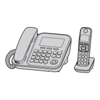
KX-TG2853BXS/KX-TG2854BXS/KX-TGA280BXS
4.2. Circuit Operation (Base Unit)
4.2.1. Outline
Base Unit consists of the following ICs as shown in Block Diagram (Base Unit) (P.7).
• BBIC (Base Band IC): IC1
- Handling all the audio, signal and data processing needed in a FHSS base unit
- Controlling the FHSS specific physical layer and radio section (Burst Module Controller section)
- ADPCM codec filter for speech encoding and speech decoding (DSP section)
- Echo-cancellation and Echo-suppression (DSP section)
- Any tones (tone, sidetone, ringing tone, etc.) generation (DSP section)
- DTMF receiver (DSP section)
- Clock Generation for RF Module
- ADC, DAC, timer, and power control circuitry
- All interfaces (ex: RF module, LED, Analog Front End, etc.)
• RF Module: IC701
- Transceiver IC including LNA, PLL, demodulator, logic
- PA (TX power amplifier)
• FLASH MEMORY: IC501
- Voice Prompt (TAM) D/L Area
• Additionally
- Power Supply Circuit (+3.45V, +3.0V, +1.8V output)
- Crystal Circuit (10.368MHz)
- Charge Circuit
- Telephone Line Interface Circuit
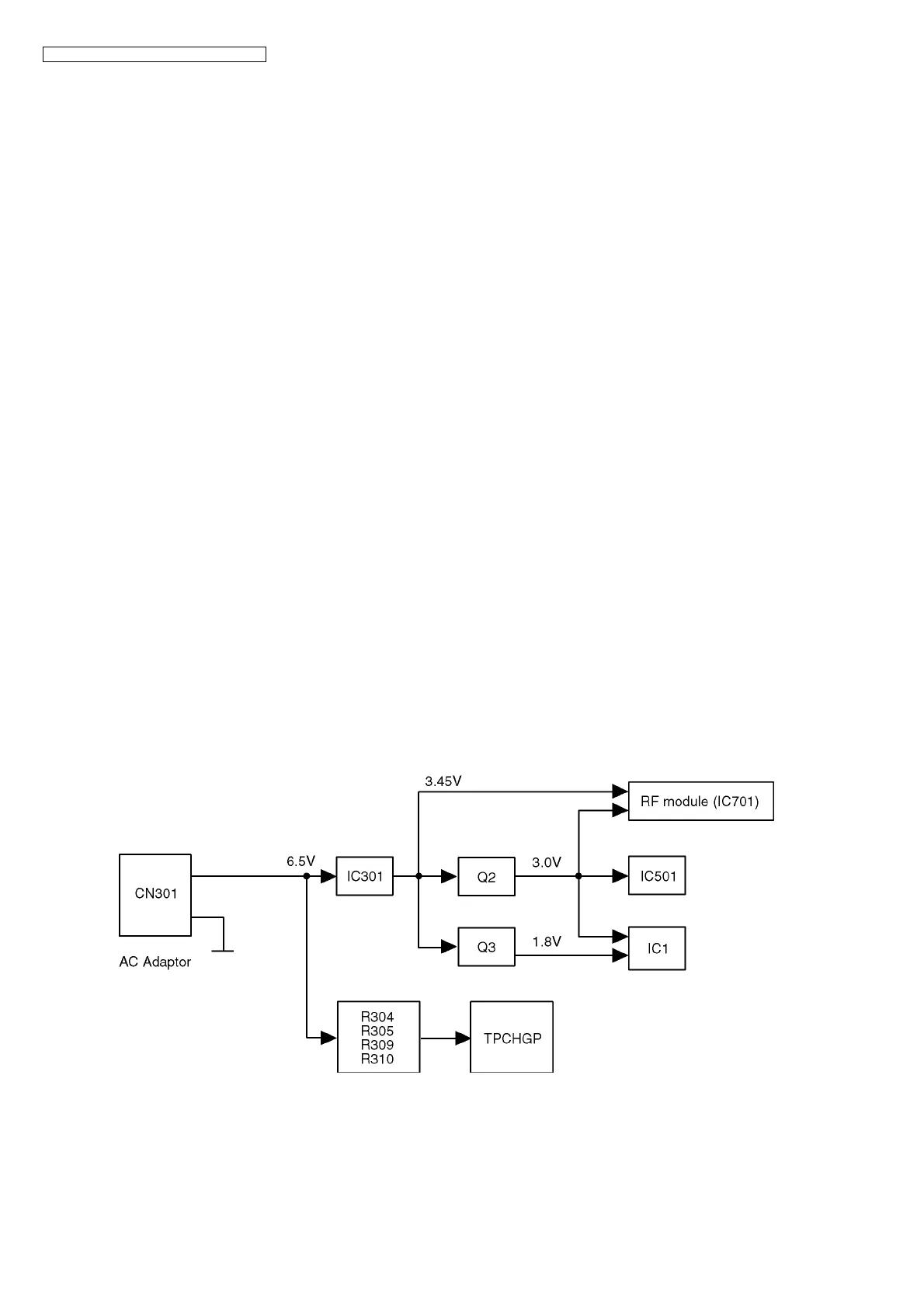
4.2.2. Power Supply Circuit
The power is supplied to the Base Band IC, RF Module and Charge Contact from AC Adaptor (+6.5V) as shown in Fig.101. The
power supply is as follows:
• Base Band IC (IC1):
CN301 (+6.5V) → IC301 → Q2 → IC1
• RF Module (IC701):
CN301 (+6.5V) → IC301 → Q2 → IC701 (PLL)
CN301 (+6.5V) → IC301 → IC701 (Power AMP)
• FLASH MEMORY (IC501):
CN301 (+6.5V) → IC301 → Q2 → IC501
• Charge Contact (TPCHGP):
CN301 (+6.5V) → R304, R305, R309, R310 → TPCHGP
<Fig.101>
 Loading...