
L
liupamelaAug 2, 2025
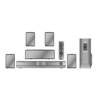
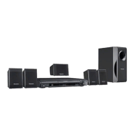
What to do if my Panasonic SA-PT460 triggers 'F61' after being on for a while?
- SSophia RosarioAug 2, 2025
If your Panasonic Home Theater System powers on for a while and then triggers an 'F61' error, try these steps: First, re-connect the Fan to CN5501. Then, check the fan circuit, specifically components Q5640, Q5641, Q5642, and Q5644. Next, touch up any solder crack areas or replace any defective parts, especially Q5860, Q5861, Q5862, TH5860 (temperature detection components), QR5801, and QR5802 (30V detection components). Finally, inspect the feedback circuit, including IC5801, PC5720, and D5725, replacing any faulty components.