Circuit Descriptions, Abbreviation List, and IC Data Sheets
EN 61LC8.1E LB 9.
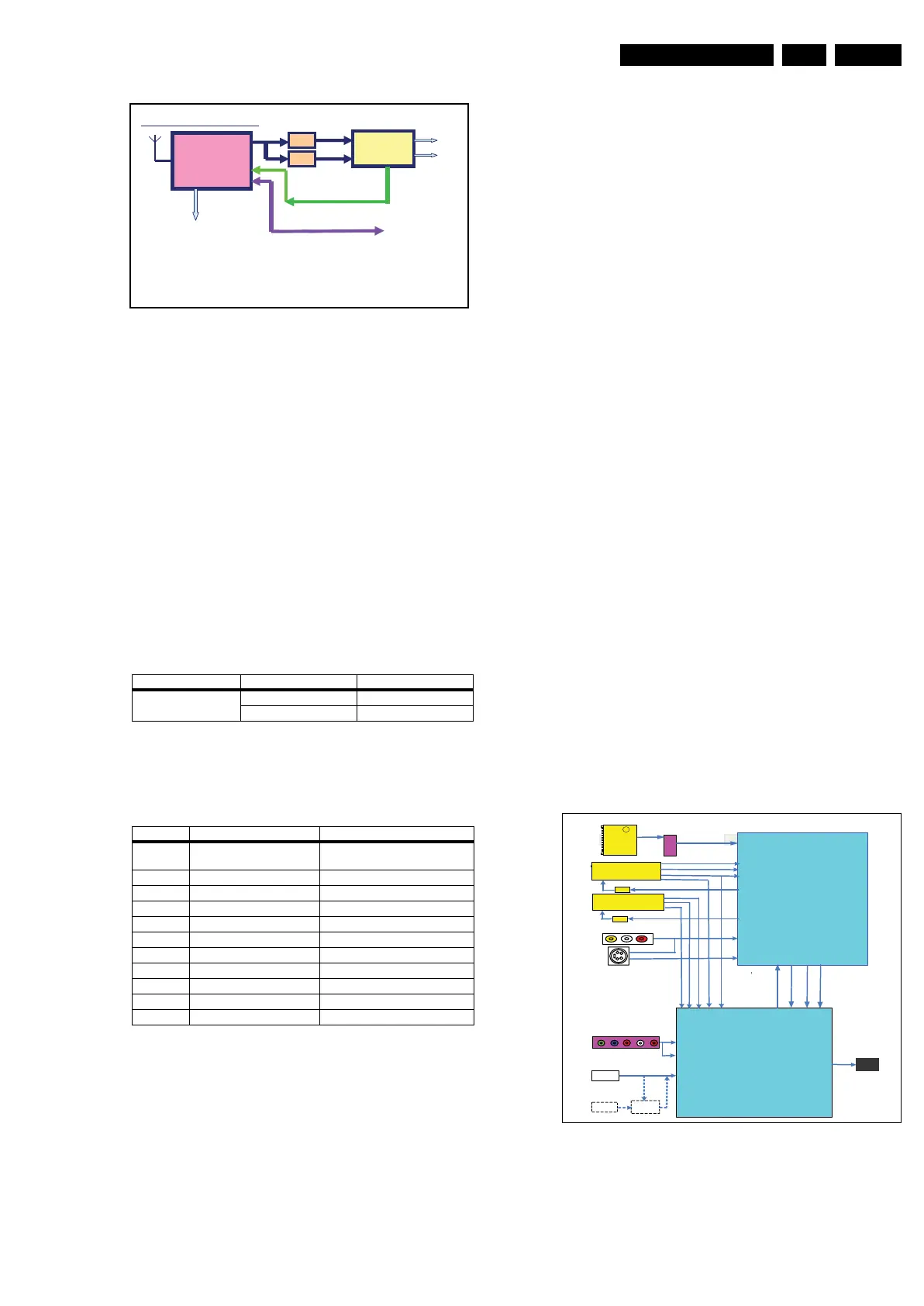
Figure 9-10 Tuner IF diagram
While receiving analogue signals, the signal coming from the
tuner is fed to the IF demodulator (through the SAW filters) and
then passed to the NXP TDA8890H1 LOC-TOP Front-End
Signal Processor.
9.4.1 Video IF Amplifier
The IF-filter is integrated in a SAW (Surface Acoustic Wave)
filter. One for filtering IF-video (item 1102) and one for IF-audio
(item 1103). The video IF filter can be switched to another
standard, what makes it suitable for applications in multi-
standard platforms (implemented in non-EU applications).
If implemented, switching is done by the microcontroller via
SAW_SW. In table “SAW filter switching” is explained how to
address the different system standards.
Table 9-1 SAW filter switching
The pin assignment of all analogue tuners is equal and can be
found in table “Pin assignment analogue tuners”.
Table 9-2 Pin assignment analogue tuners
9.5 Video/Audio Processing
The video and audio processing is handled by the NXP “LOC-
TOP” TDA8890H1 front-end signal processor in cooperation
with the NXP “LOC-TOP” TDA15471HV video/audio
processor. For the applications, see figures “Block diagram
video processing” and “Block diagram audio processing”.
The TDA8890H1 features:
• Multi-standard vision IF circuit with alignment-free PLL
demodulator
• Internal (switchable) time-constant for the IF-AGC circuit
• Switchable group delay correction and sound trap (with
switchable centre frequency) for the demodulated CVBS
signal
• Separate SIF (Sound IF) input for single reference QSS
(Quasi Split Sound) demodulation
• AM demodulator without extra reference circuit
• SSIF output is available for interfacing with a stereo sound
decoder
• Audio switch circuit with 7 base band stereo sound inputs
• Audio switch circuit 3 stereo outputs
• Video switch with 4 external CVBS inputs
• Video switch with 3 CVBS outputs
• YPRPB outputs (YOUTPIP/PBOUTPIP/PROUTPIP), for
back-end PIP processing
• Linear RGB/YPBPR input with fast insertion
• Video identification circuit
• One reference (24.576 MHz) clock required
• Indication of the Signal-to-Noise ratio of the incoming
CVBS signal
• Horizontal synchronization with alignment-free horizontal
oscillator
• Vertical count-down circuit to generate vertical timing
signals.
The TDA15471HV features:
• Graphics and Video Input Ports
• HDMI receiver
• 3D Video Decoder
• Field-proven Multi-standard TV sound decoder
• Audio processor
• Analog sound interface
• Digital audio input and output interface
• High Quality Video Processing
• Pip and PoP
• High Quality Video Scaling Engine
• Embedded OSD and VBI Controller
• Embedded DDR/SDRAM controller
• Programmable Digital Output for LCD
• Powerful 32-bit RISC CPU.
9.5.1 Video/Audio Application
“Block diagram video processing” and “Block diagram audio
processing” shows the video/audio signal flow.
Figure 9-11 Block diagram video processing
Region SAW_SW System
AP 1 B/G, D/K, I
0M/N
Pin number Description DC voltage (V)
1 RF AGC voltage 3.3 - 4.5 (weak or no signal)
< 3.3 (strong signal)
2n.c.
3I
2
C-bus address select 0
4 SCL 0 to 3.3
5 SDA 0 to 3.3
6n.c.
7 supply voltage 5 ±0.25
8n.c.
9 fixed tuning voltage 33
10 n.c.
11 TV IF output
Tuner IF Diagram
CVBS
2
nd
SIF
tuner
Video
SAW filter
Audio
SAW filter
IF demodulator
RFAGC
RF
AGC_analog
IIC
Supply
+5V/+33V
IIC_analog
I_17820_035.eps
130308
L
R
Y
Pb
Pr
HDMI 1
HDMI 2
Ext 1 - Scart 1
SMIC
TDA8890
LOC TOP
TDA15471/15421
Tuner
=
CVB
S
L
R
SAW
HDMI
MUX
Ext 2 - Scart 2
VIFIN1,VIFIN2
72,71
1102
CVBS4/Y4,50
VIDOUTS2
39
CVBS2, 27
Y2,PB2,PR2,15,17,18 Y,PB,Pr,OUTPIP24,23,25
CVBS2/Y2,46
VIF1,2
SC1_CVBS_IN
SC1_R, G, B_IN
SC2 _Y _CV BS_ IN
CVBSOUT,30
R3/PR3/Y3, G3/Y3/CVBS3, B3/PB3,30,29,28
INSSW3 ,31
7503
SC1_FBL_IN
SC1_RF_OUT_CVBS
VIDOUTs1
53
SC2_CVBS_MON_OUT
7E01
SVHS_Y_CVBS_IN
SVHS_C_IN
CVBS5/Y5
44
C2/C4/C5
42
SC2_C_IN
C2,26
MON_CVBS
SOG,4
FS3,23
FB2,16
SC2_STATUS
SC1 _S TAT US
SC1_FBL_IN
PIP_R,G,B
MAIN_CVBS_Y
MAIN_C
MAINVIDOUT,16
MAINCOUT,17
CVB S1, 25
C1,24
Y1, PB1,PR1
9,10 ,11
SOY1,9
LVDS
RXC P,M 233 ,232 ;
RX , P,M 237 ,236 ,241 ,240 ,245 ,244
HDMI_MUX_TX +, -
I_18170_047.eps
310708