Circuit Descriptions
EN 56 Q552.2L LA7.
2012-Mar-16
back to
div. table
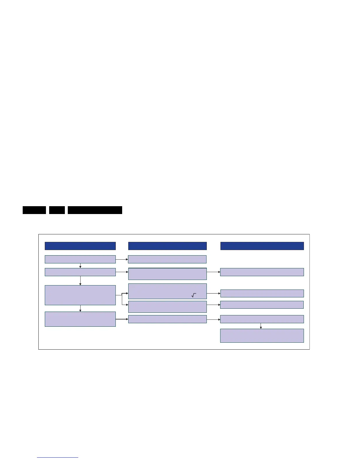
Figure 7-4 Test instructions
Following checks have to be performed:
• check fuse (F101)
• standby check V
STB
(C306), measure 3.3 V
• PFC voltage check (C644), measure 380 - 400 V; if no PFC
applied, measure 311 @ 220 V
• multi-level check V
SSB
(C208), measure 12.3 V
• multi-level check V
SND
(C233), measure 24.5 V
• reference voltage check (U401), measure 12 V (appr.).
SAFETY INSTRUCTION
Replace safety components, indicated by the symbol h, only
by components identical to the original ones. Any other
component substitution (other than original type) may increase
risk of fire or electrical shock hazard.
7.3 DC/DC Converters
The on-board DC/DC converters deliver the following voltages
(depending on set execution):
• +3V3-STANDBY, permanent voltage for the Stand-by
controller, LED/IR receiver and controls; connector 1M95
pin 1
• +12V, input from the power supply for TV550 common
(active mode); connector 1M95 pins 6, 7 and 8
• +24V, input from the power supply for DVB-S2 (in active
mode); connector 1M09 pins 1 and 2
• +1V1, core voltage supply for PNX855xx; has to be started
up first and switched "off" last (diagram B03B)
• +1V2, supply voltage for analogue blocks inside PNX855xx
• +1V8, supply voltage for DDR2 (diagram B03B)
• +2V5, supply voltage for analogue blocks inside PNX855xx
(see diagram B03E)
• +3V3, general supply voltage (diagram B03E)
• +5V, supply voltage for USB and CAM (diagram B03E)
• +5V-TUN, supply voltage for tuner (diagram B03E)
• +V-LNB, input voltage for LNB supply IC (item no. 7T50)
• +5V-DVBS, input intermediate supply voltage for DVB-S2
(diagram B08A)
• +3V3-DVBS, clean voltage for silicon tuner and DVB-S2
channel decoder
• +2V5-DVBS, clean voltage for DVB-S2 channel decoder
• +1V-DVBS, core voltage for DVB-S2 channel decoder.
A +12 V under-voltage detector (see diagram B03C) enables
the 12V to 3.3V and 12V to 5V DC/DC converters via the
ENABLE-3V3-5V line, and the 12V to 1.8V DC/DC converter
via the ENABLE-1V8 line. DETECT2 is the signal going to the
Stand-by microcontroller and ENABLE-3V3n is the signal
coming from the Stand-by microcontroller.
Diagram B03D contains the following linear stabilizers:
• +2V5 stabilizer, built around item no. 7UCO
• +5V-TUN stabilizer, built around items no. 7UA6 and 7UA7
• +1V2 stabilizer, built around items no. 7UA3 and 7UA4.
Diagram B08A contains the DVB-S2-related DC/DC
converters and -stabilizers:
• a +24V under-voltage detection circuitry is built around
item no. 7T04
• the switching frequency of the 24 to 14...20V switched
mode converter is 350 kHz (item no. 7T03 and +V-LNB
lines)
• the output signal on the +V-LNB line goes to the LNBH23Q
(item no. 7T50)
• the LNBH23Q (item no. 7T50) sends a feedback signal via
the V0-CNTRL line
• the switching frequency of the +5V-DVBS to +1-DVBS
switched mode converter is 900 kHz (item no. 7T00)
• a delay line for the +2V5-DVBS and +1V-DVBS lines is
created with item no. 3T03 (R=10k) and 2T06 (C=100n)
• a 3.3V to 2.5V linear stabilizer is built around item no. 7T01
• a 5V to 3.3V linear stabilizer is built around item no. 7T02.
Diagram B08B contains the DVB-S2 LNB supply:
• the +V-LNB signal comes from item no. 7T03
• the V0-CTRL signal goes to item no. 7T03
• the LNB-RF1 goes to the LNB.
Figures gives a graphical representation of the DC/DC
converters with its current consumptions:
19132_013_111221.eps
111222
Normal operation
Apply the mains voltage (AC
in
)
Pull the Standby pin to LOW (GND)
Pull the BL_ON_OFF pin to HIGH (3.3 V)
Check the main supply at C208: measure 12.3 V
Check the audio supply at C233: measure 24.5 V
Check the PFC voltage at C644
PFC present: measure 380 V to 400 V
PFC not present: measure ACin × 2
No turn on
Check First step Second step
Check the entire block (PC102, V
CC
, etc.)
Check the entire block (V
CC
, ICs, etc.)
Allow the power supply to start-up a few times
Check the Standby voltage
at C306: measure 3.3 V
Check the reference voltage of the
LED Driver (U401): measure approximately 12 V
Check the fuse (F101)
Check the entire block (V
CC
, ICs, etc.)