TDA8950_2 © NXP B.V. 2009. All rights reserved.
Product data sheet Rev. 02 — 11 June 2009 7 of 39
NXP Semiconductors
TDA8950
2 × 150 W class-D power amplifier
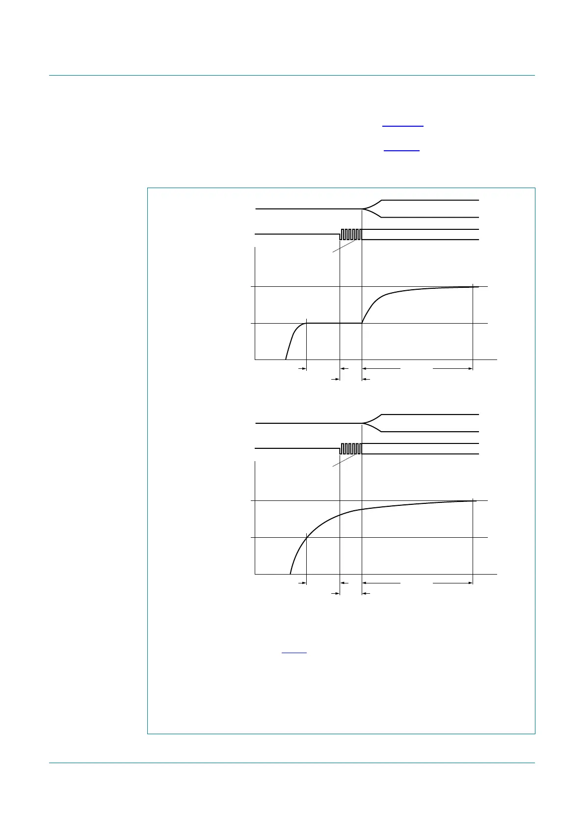
To ensure the coupling capacitors at the inputs (C
IN
in Figure 10) are fully charged before
the outputs start switching, a delay is inserted during the transition from Mute to Operating
mode. An overview of the start-up timing is provided in Figure 5. For proper switch-off, the
MODE pin should be forced LOW at leaxt 100 ms before the supply lines (V
DDA
and V
SSA
)
drop below 12.5 V.
(1) First
1
⁄
4
pulse down.
Upper diagram: When switching from Standby to Mute, there is a delay of approximately 100 ms
before the output starts switching. The audio signal will become available once V
MODE
reaches the
Operating mode level (see Table 8), but not earlier than 150 ms after switching to Mute. To start-up
pop noise-free, it is recommended that the time constant applied to pin MODE be at least 350 ms
for the transition between Mute and Operating modes.
Lower diagram: When switching directly from Standby to Operating mode, there is a delay of
100 ms before the outputs start switching. The audio signal becomes available after a second
delay of 50 ms. To start-up pop noise-free, it is recommended that the time-constant applied to pin
MODE be at least 500 ms for the transition between Standby and Operating modes.
Fig 5. Timing on mode selection input pin MODE
2.2 V < V
MODE
< 3 V
audio output
operating
standby
mute
50 %
duty cycle
> 4.2 V
0 V (SGND)
time
001aah657
V
MODE
100 ms
50 ms
modulated PWM
> 350 ms
2.2 V < V
MODE
< 3 V
audio output
operating
standby
mute
50 %
duty cycle
> 4.2 V
0 V (SGND)
time
V
MODE
100 ms
50 ms
modulated PWM
> 350 ms
(1)
(1)