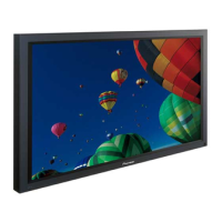
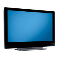
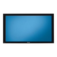
PDP-433PU
106
1234
1234
C
D
F
A
B
E
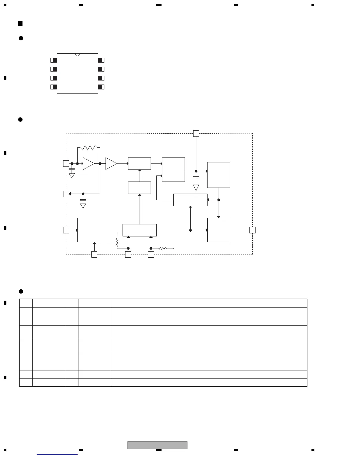
Pin Assignment (Top View)
Pin Function
Block Diagram
FS781BZB (DIGITAL VIDEO ASSY: IC1802)
Low EMI Clock IC
1
2
3
4
8
7
6
5
Xin
Xout
S1
LF
VDD
S0
FSOUT
VSS
FS78x
8 Pin SOIC Package
Phase
Detector
VCO
1(3)
2(4)
Xin
Xout
10 pF.
Reference
Divider
8 pF
8 pF
250 K
VCO / N
Modulation
Control
Input Control Logic
Output
Divider
and
Mux
Power Contol
Logic
3(5)
7(1)
8(2)
5(7)
4(6)
VDD
S0S1
FSOUT
Loop Filter
VSS
6(8)
VSS
VDD
(TSSOP Pin #)
No. Pin Name I/O Type Function
1/2 Xin/Xout I/O Analog
Pins form an on-chip reference oscillator when connected to terminals of an external parallel
resonant crystal. Xin may be connected to TTL/CMOS external clock source. If Xin connected
to external clock other than crystal, leave Xout (pin2) unconnected.
7/3 S0/S1 I CMOS/TTL
Digital control inputs to select input frequency range and output frequency scaling. Refer to
Tables 7 and 8 for selection. S0 has internal pulldown. S1 has internal pullup.
4LFIAnalog
Loop Filter. Single ended tri-state output of the phase detector. A two-pole passive loop filter
is connected to Loop Filter (LF).
6 FSOUT O CMOS/TTL
Modulated Clock Frequency Output. The center frequency is the same as the input reference
frequency for FS781. Input frequency is multipled by 2X and 4X for FS782 and FS784
respectively.
8 VDD P Power
Positive Power Supply
5 VSS P Power
Power Supply Ground
 Loading...