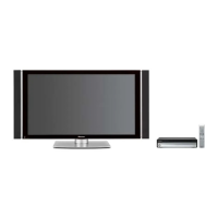
PDP-5016HD
207
5678
56
7
8
C
D
F
A
B
E
Pin Function
PIN
NO
1NC
2 P3_5/SCL/SSCK SCL(I2C) I2C clock I
3 P3_3/SSI
4 P3_4/SDA/SCS SDA(I2C) I2C data I/O
5 MODE
6 P4_3/XCIN
7 P4_4/XCOUT
8 RESET RESET
9 P4_7/XOUT XOUT O
10 VSS/AVSS VSS
11 P4_6/XIN XIN
Output for the main clock
Input for the main clock I
12 VCC/AVCC VCC
13 P2_7/TRDIOD1 ID7 I2C device ID setting 7 I
14 P2_6/TRDIOC1 ID6 I2C device ID setting 6
15 P2_5/TRDIOB1 ID5 I2C device ID setting 5
16 P2_4/TRDIOA1 ID4 I2C device ID setting 4
17 P2_3/TRDIOD0 ID3 I2C device ID setting 3
18 P2_2/TRDIOC0 ID2 I2C device ID setting 2
19 P2_1/TRDIOB0 ID1 I2C device ID setting 1
I
I
I
I
I
I
20 P2_0/TRDIOA0
21
P1_7/TRAIO/INT1
22 P1_6/CLK0 Md_REQ_IN Input of REQ signal from Md I
23 P1_5/RXD0 RXD0
Receiving of UART communication data with Md microcomputer
I
24 P1_4/TXD0 TXD0
Transmission of UART communication data with Md microcomputer
O
25 P1_3/KI3/AN11 STATUS Md error output O
26 NC
27 P4_5/INT0 REQ_OUT REQ signal outout O
L
H
28 P6_6/INT2/TXD1 TXD1
Transmission of UART communication data with the PC
O
29 P6_7/INT3/RXD1 RXD1
Receiving of UART communication data with the PC
I
30 P1_2/KI2/AN10 POWER Power ON/OFF switching I
31 P1_1/KI1/AN9 MAX_PLS11 4L/2L switching 1
32 P1_0/KI0/AN8 MAX_PLS10 4L/2L switching 0
I
I
33 P3_1/TRBO MASK1 Mask pattern switching 1
34 P3_0/TRAO MASK0 Mask pattern switching 0
I
I
35 P6_5/CLK1 DITHER Dither switching I
36 P6_4
37 P6_3
38 P0_7/AN0 AC_OFF AC input detection I H
39 NC
40 NC
41 P0_6/AN1 MAX_PLS21 Peak brightness switching 1
42 P0_5/AN2 MAX_PLS20 Peak brightness switching 0
43 P0_4/AN3 RS_SEL2 Data conversion switching 2
I
I
I
44 P4_2/VREF VCC I
45 P6_0/TREO
46 P6_2
47 P6_1 ZAC Aging mode switching I
48 P0_3/AN4 RS_SEL1 Data conversion switching 1
49 P0_2/AN5 RS_SEL0 Data conversion switching 0
I
I
50 P0_1/AN6 MSEL GPIO/I2C conversion switching I
51 P0_0/AN7 CHSEL Operational mode setting I
52 P3_7/SSO
I
(fixed to
Initial setting
at power ON
Pin name Signal name Function
input)
ActiveI/O
w
w
w
.
x
i
a
o
y
u
1
6
3
.
c
o
m
Q
Q
3
7
6
3
1
5
1
5
0
9
9
2
8
9
4
2
9
8
T
E
L
1
3
9
4
2
2
9
6
5
1
3
9
9
2
8
9
4
2
9
8
0
5
1
5
1
3
6
7
3
Q
Q
TEL 13942296513 QQ 376315150 892498299
TEL 13942296513 QQ 376315150 892498299
http://www.xiaoyu163.com
http://www.xiaoyu163.com
 Loading...