66
PDP-503PE, PDP-503PU
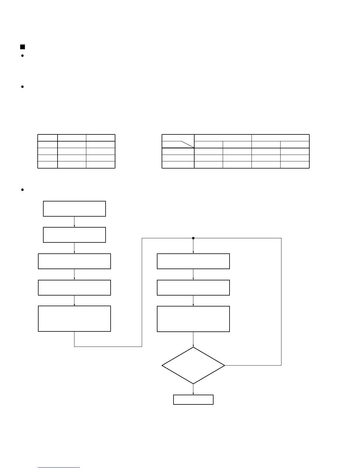
Timing Adjustment of X and Y DRIVE Assys Control Signal
As for this adjustment, adjustment with set state is difficult.
Therefore replace it every Assy when replacing the pulse module.
Adjustment VR Test pin for adjustment and measurment
Display a SUSOUT waveform
Power ON and display a SUSOUT
waveform
Display a SUS-D waveform
Display a SUS-U waveform
Power ON and
display a SUS-D waveform
Display a SUS-U waveform
Measuring points of waveform
are refered to next page.
Power ON
Black Mask Screen
Coarse adjustment of
SUS-U, SUS-B, SUS-G
SUS-D adjustment
Adjust the waveform to 20-25ns.
SUS-U adjustment
Adjust the waveform to 20-25ns.
Power OFF
Compare waveform,
and do harmonize
almost?
Yes
No
Adjust VR resistance value
of SUS-B and SUS-G to match
VR resistance value of SUS-D
within ± 2Ω.
Adjust VR resistance value
of SUS-B and SUS-G to match
VR resistance value of SUS-D
within ± 2Ω.
Power OFF
Adjustment end
SUS-D readjustment
Adjust the waveform to 20-25ns.
SUS-U readjustment
Adjust the waveform to 20-25ns.
X DRIVE Y DRIVE
SUS-U VR3203 VR2204
SUS-D VR3202 VR2203
SUS-B VR3201 VR2202
SUS-G VR3200 VR2201
Pulse Module X DRIVE Y DRIVE
Upper Lower Upper Lower
SUSOUT K3105 K3106 K2212 K2203
SUS-U K3200 K3204 K2220 K2224
SUS-D K3108 K3205 K2207 K2225
Purpose
• Pulse module loads in DRIVE Assy as one of heat measures of DRIVE Assy. Adjust the drive timing of the pulse module
driving parallel with VR.
• Pulse module has each peculiar delay time. Readjustment is necessary when replaced the pulse module in the X and
Y DRIVE Assys.
Adjustment Method
CR delay circuit is each inserted on signal path of four control signals (SUS-U, SUS-B, SUS-D, SUS-G) driving
the pulse module.
Quantity of delay can adjust pulse module of one side with VR.
Adjust VR while measuring a waveform of the pulse module, and match a timing.
Adjustment Procedure
 Loading...