37
6. Technical Information
6.1 Introduction
This section contains a description of the PI 4100’s circuits with reference to its printed circuit boards as
shown on the System Block Diagram, Fig. 1, p. 10. This is followed by schematic diagrams and
component layout drawings for the printed circuit boards manufactured by Potomac Instruments.
6.2 PI 4100 Technical Description:
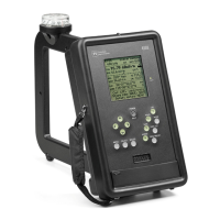
The PI 4100’s circuitry is contained on six printed circuit boards (pcbs), which are designated the
Antenna, Receiver, Power/Audio, CPU, Display, and GPS pcbs. The pcbs are all interconnected by short
ribbon cables. The following paragraphs describe the circuits found on each pcb.
Antenna: The PI 4100 uses a multiturn loop antenna, balanced to ground, formed on a printed-circuit
board which is encapsulated in molded plastic. It works into a balanced low-impedance receiver input
circuit (on the receiver pcb) for which the signal level to the receiver for a given field strength is nearly
constant in the working frequency range. Around the receiving loop antenna on the pcb is a separate
single-turn loop to which a calibrating current is fed to generate a calibrating field for self-calibration.
Both loops are connected to the receiver pcb by a short ribbon cable.
Receiver: On the receiver pcb the balanced-to-unbalanced receiver input circuit feeds a low-noise, low-
distortion broadband RF amplifier which drives the receiver mixer and supplies an external RF output. A
frequency synthesizer generates the local oscillator signal for the mixer in 1 kHz steps under the control
of the central microcontroller (cpu) and the front-panel keys. The balanced mixer up-converts the
selected RF signal to an IF frequency of 10.703 MHz. At this frequency the signal passes through a
4 kHz bandpass crystal filter which gives high adjacent-channel rejection. The filter output drives a
three-stage variable-gain IF amplifier for which the gain in dB varies linearly with control voltage. A
second crystal filter between two amplifier stages narrows the measuring bandwidth to 1.0 kHz. A
detector at the amplifier output is forced to have a constant output by having its output control the
amplifier gain, so that the amplifier gain control voltage is proportional to the received field strength (in
dBuV/m) and is the output to the measuring circuits on the cpu pcb.
Calibration signal source: Also on the receiver pcb, a calibration signal at the RF frequency is
generated in a second balanced mixer for which the inputs are (1) the local oscillator synthesizer which
also drives the receive mixer, and (2) a 10.703 MHz crystal oscillator. The frequency difference between
these inputs is the RF frequency to which the receiver is set. The mixer provides balanced current-source
outputs directly to the two terminals of the calibrating loop on the antenna pcb. The source is switched on
only for 700 milliseconds during the calibration cycle under the control of the cpu, as described in Sec.
4.2.3, p. 20.
Power/Audio: This pcb contains the battery charge control IC, with protection circuits and a linear
regulator at its input. The battery feeds a second linear regulator to provide the main +5 Volt supply.
This in turn drives a dc-dc converter, operating at 5.4 MHz to avoid signal interference, which has outputs
at -5 Volts and -17 Volts. There is also a “class D” audio power amplifier to drive the speaker with high
efficiency.
CPU: This pcb receives outputs from, and sends inputs to, all other boards. It contains the main
microcontroller for the unit; the main memory IC; the USB interface IC; audio response shaping circuits;
a 3.3 Volt linear voltage regulator; a signaling buzzer; and various switching transistors. The
microcontroller controls the frequency synthesizer, the memory IC, and the USB IC by means of an SPI
bus. It directly controls the display, the buzzer, and supply voltage switching. From the front panel key