LTE Standard Module Series
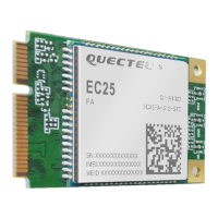
EC25 Hardware Design
EC25_Hardware_Design 24 / 130
5. Pins 119~126 and 128 are used for SGMII interface.
6. Pins 24~27 for PCM function are multiplexing pins used for audio design on EC25 module and BT
function on FC20 module.
7. SD card, wireless connectivity and SGMII interfaces (pins 37~40, 118, 127, 129~139, 119~126, 128,
23, 28~34) are not supported on ThreadX modules.
8. Keep all RESERVED pins and unused pins unconnected.
9. GND pins 85~112 should be connected to ground in the design. RESERVED pins 73~84 should not
be designed in schematic and PCB decal, and these pins should be served as a keepout area.
3.3. Pin Description
The following tables show the pin definition of EC25 module.
Table 3: I/O Parameters Definition
Table 4: Pin Description
Type Description
AI Analog Input
AO Analog Output
DI Digital Input
DO Digital Output
IO Bidirectional
OD Open Drain
PI Power Input
PO Power Output
Power Supply
Pin Name Pin No. I/O Description DC Characteristics Comment
VBAT_BB 59, 60 PI
Power supply for
module’s baseband
part
Vmax=4.3V
Vmin=3.3V
Vnorm=3.8V
It must be provided with
sufficient current up to
0.8A.