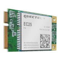
LTE Standard Module Series
EC25 Hardware Design
EC25_Hardware_Design 28 / 130
DBG_TXD 12 DO Transmit data
V
OL
max=0.45V
V
OH
min=1.35V
1.8V power domain.
If unused, keep it
open.
DBG_RXD 11 DI Receive data
V
IL
min=-0.3V
V
IL
max=0.6V
V
IH
min=1.2V
V
IH
max=2.0V
1.8V power domain.
If unused, keep it
open.
ADC Interfaces
Pin Name Pin No. I/O Description DC Characteristics Comment
ADC0 45 AI
General purpose
analog to digital
converter
Voltage range:
0.3V to VBAT_BB
If unused, keep it
open.
ADC1 44 AI
General purpose
analog to digital
converter
Voltage range:
0.3V to VBAT_BB
If unused, keep it
open.
PCM Interface
1)
Pin Name Pin No. I/O Description DC Characteristics Comment
PCM_IN 24 DI PCM data input
V
IL
min=-0.3V
V
IL
max=0.6V
V
IH
min=1.2V
V
IH
max=2.0V
1.8V power domain.
If unused, keep it
open.
PCM_OUT 25 DO PCM data output
V
OL
max=0.45V
V
OH
min=1.35V
1.8V power domain.
If unused, keep it
open.
PCM_SYNC 26 IO
PCM data frame
synchronization
signal
V
OL
max=0.45V
V
OH
min=1.35V
V
IL
min=-0.3V
V
IL
max=0.6V
V
IH
min=1.2V
V
IH
max=2.0V
1.8V power domain.
In master mode, it is
an output signal.
In slave mode, it is an
input signal.
If unused, keep it
open.
PCM_CLK 27 IO PCM clock
V
OL
max=0.45V
V
OH
min=1.35V
V
IL
min=-0.3V
V
IL
max=0.6V
V
IH
min=1.2V
V
IH
max=2.0V
1.8V power domain.
In master mode, it is
an output signal.
In slave mode, it is an
input signal.
If unused, keep it
open.
I2C Interface