LTE Standard Module Series
EC25 Hardware Design
EC25_Hardware_Design 55 / 130
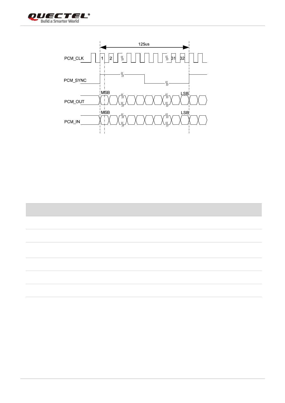
Figure 23: Auxiliary Mode Timing
The following table shows the pin definition of PCM and I2C interfaces which can be applied on audio
codec design.
Table 14: Pin Definition of PCM and I2C Interfaces
Clock and mode can be configured by AT command, and the default configuration is master mode using
short frame synchronization format with 2048KHz PCM_CLK and 8KHz PCM_SYNC. Please refer to
document [2] for more details about AT+QDAI command.
The following figure shows a reference design of PCM interface with external codec IC.
Pin Name Pin No. I/O Description Comment
PCM_IN 24 DI PCM data input 1.8V power domain
PCM_OUT 25 DO PCM data output 1.8V power domain
PCM_SYNC 26 IO
PCM data frame
synchronization signal
1.8V power domain
PCM_CLK 27 IO PCM data bit clock 1.8V power domain
I2C_SCL 41 OD I2C serial clock Require external pull-up to 1.8V
I2C_SDA 42 OD I2C serial data Require external pull-up to 1.8V