LTE Standard Module Series
EC25 Hardware Design
EC25_Hardware_Design 63 / 130
Table 19: Pin Definition of SGMII Interface
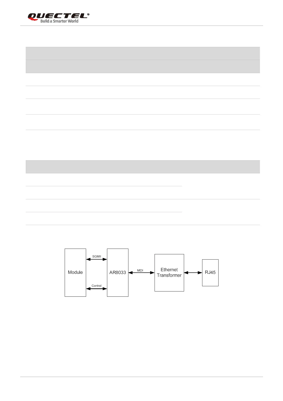
The following figure shows the simplified block diagram for Ethernet application.
Figure 27: Simplified Block Diagram for Ethernet Application
The following figure shows a reference design of SGMII interface with PHY AR8033 application.
Pin Name Pin No. I/O Description Comment
Control Signal Part
EPHY_RST_N 119 DO Ethernet PHY reset 1.8V/2.85V power domain
EPHY_INT_N 120 DI Ethernet PHY interrupt 1.8V power domain
SGMII_MDATA 121 IO
SGMII MDIO (Management Data
Input/Output) data
1.8V/2.85V power domain
SGMII_MCLK 122 DO
SGMII MDIO (Management Data
Input/Output) clock
1.8V/2.85V power domain
USIM2_VDD 128 PO SGMII MDIO pull-up power source
Configurable power source.
1.8V/2.85V power domain.
External pull-up power source for
SGMII MDIO pins.
SGMII Signal Part
SGMII_TX_M 123 AO SGMII transmission - minus
Connect with a 0.1uF capacitor,
and is close to the PHY side.
SGMII_TX_P 124 AO SGMII transmission - plus
SGMII_RX_P 125 AI SGMII receiving - plus
Connect with a 0.1uF capacitor,
and is close to EC25 module.
SGMII_RX_M 126 AI SGMII receiving - minus