LTE Module Series
EC25-V User Manual
EC25-V_User_Manual Confidential / Released 40 /
69
PCM data frame sync signal
Require external pull-up to 1.8V
Require external pull-up to 1.8V
Clock and mode can be configured by AT command, and the default configuration is master mode using
short sync data format with 2048kHz PCM_CLK and 8kHz PCM_SYNC. Refer to document [2] about the
command AT+QDAI for details.
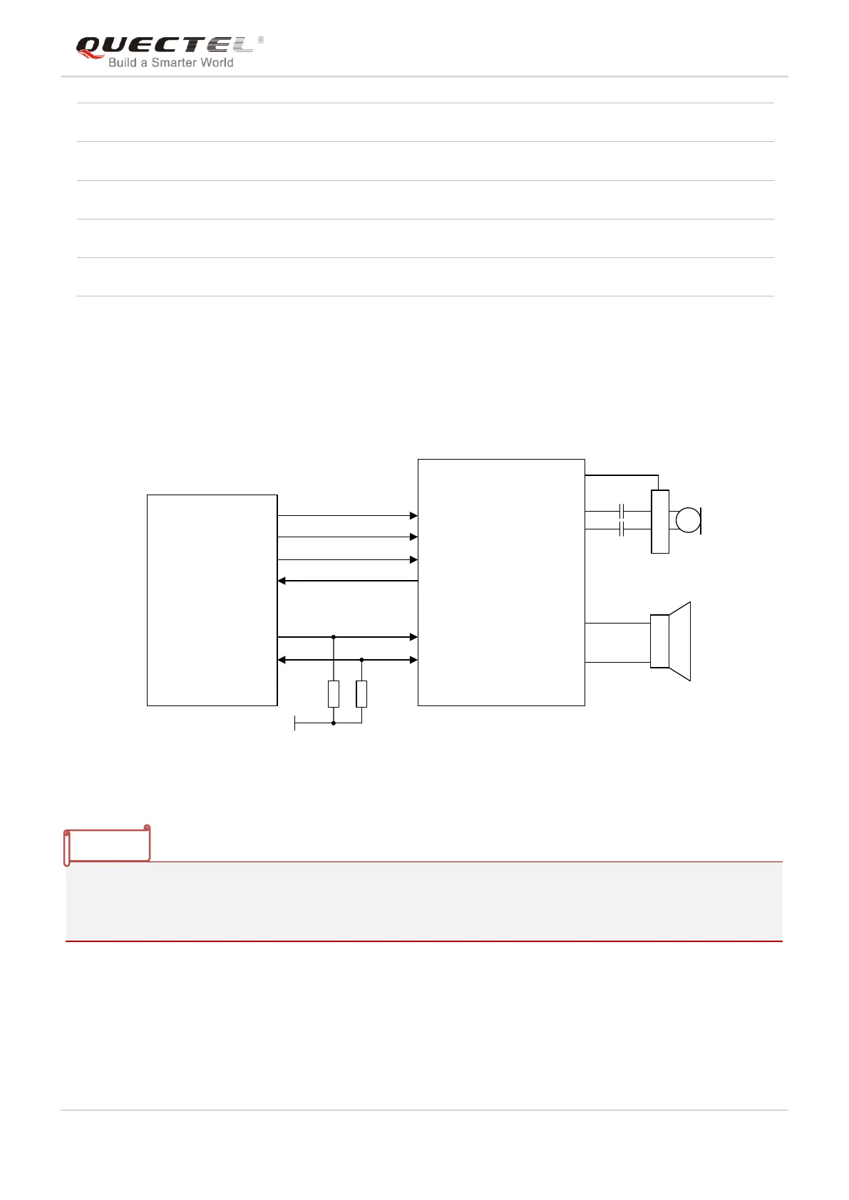
The following figure shows the reference design of PCM interface with external codec IC.
PCM_IN
PCM_OUT
PCM_SYNC
PCM_CLK
I2C_SCL
I2C_SDA
Module
1.8V
4.7K
4.7K
BCLK
LRCK
DAC
ADC
SCL
SDA
BIAS
MICBIAS
INP
INN
LOUTP
LOUTN
Codec
Figure 24: Reference Circuit of PCM Application with Audio Codec
1. It is recommended to reserve RC (R=22ohm, C=22pF) circuit on the PCM lines, especially for
PCM_CLK.
2. EC25 works as a master device pertaining to I2C interface.