LTE-A Module Series
EM06 Series Hardware Design
EM06_Series_Hardware_Design 23 / 69
3.4. Power Supply
The following table defines VCC and GND pins.
Table 6: Definition of VCC and GND Pins
3.4.1. Decrease Voltage Drop
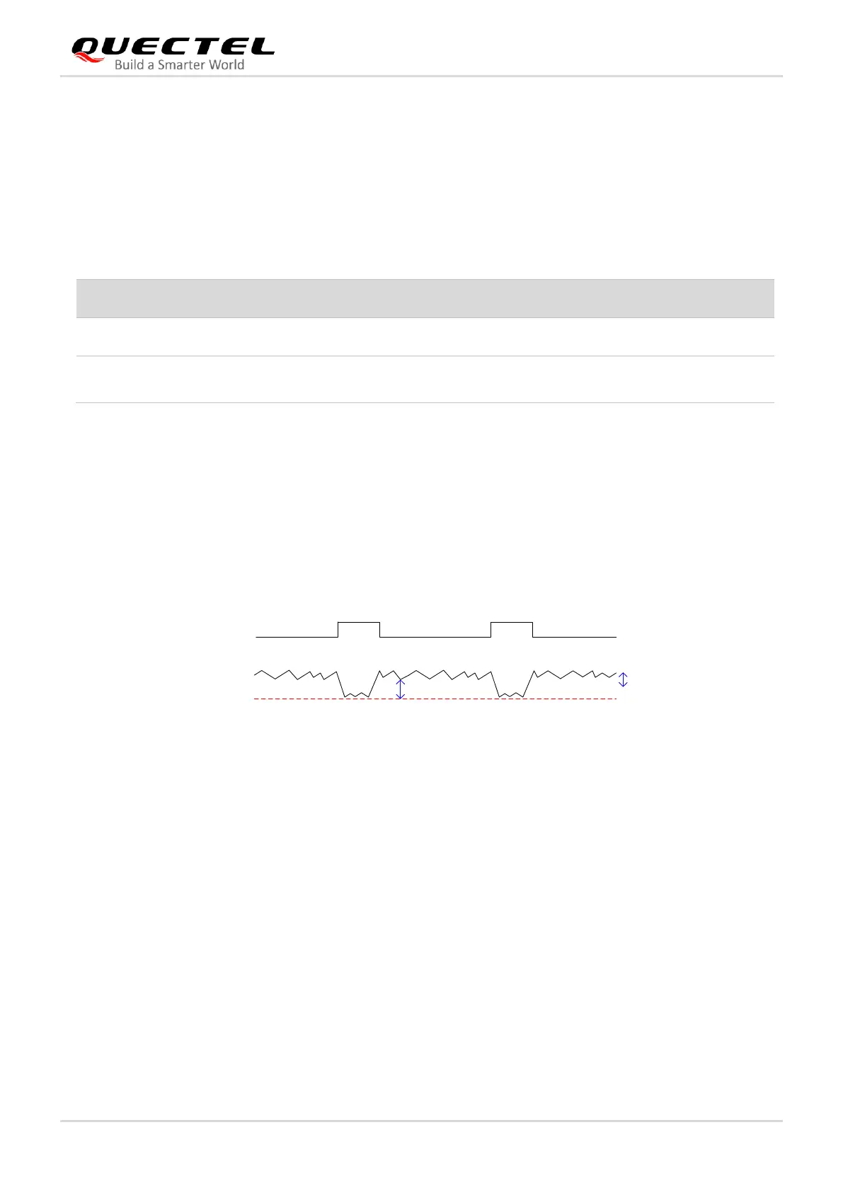
The power supply range of the module is from 3.135 V to 4.4 V. Please make sure that the input voltage
never drops below 3.135 V, otherwise the module will be powered off automatically. The following figure
shows the maximum voltage drop during radio transmission in 3G and 4G networks.
Figure 3: Voltage Drop Limits during Radio Transmission
To decrease voltage drop, a bypass capacitor of about 220 µF with low ESR (ESR = 0.7 Ω) should be
used, so does a multi-layer ceramic chip capacitor (MLCC) array for its ultra-low ESR. It is recommended
to add three ceramic capacitors (100 nF, 33 pF, 10 pF) close to VCC pins to compose the MLCC array.
The main power supply from an external application has to be the sole voltage source. The width of the
VCC trace should be no less than 2 mm. In principle, the longer the VCC trace is, the wider it should be.
In addition, in order to get a stable power source, it is recommended to use a zener diode with a reverse
zener voltage of 5.1 V and a dissipation power higher than 0.5 W. The following figure shows a reference
circuit of VCC.