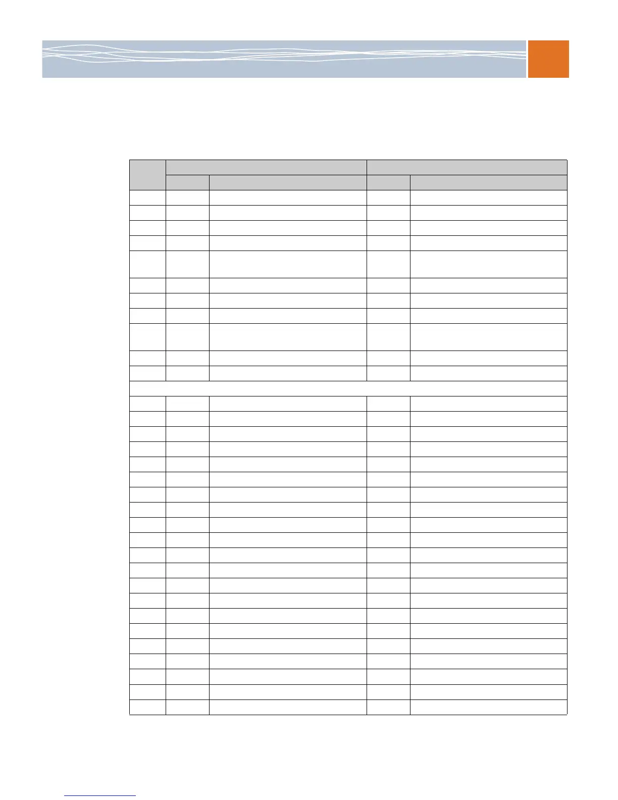
Internal device connectors
49
PCI Express x4 slot
The signals for hot plug presence detectoin in the table below are not supported on Q35
motherboards.
Pin #
Side B Side A
Signal Description Signal Description
1 +12V 12V power PRSNT1# Hot plug presence detect
2 +12V 12V power +12V 12V power
3 RSVD Reserved +12V 12V power
4 GND Ground GND Ground
5 SMCLK SMBus clock JTAG2 TCK (Test Clock), clock input for JTAG
interface
6 SMDAT SMBus data JTAG3 TDI (Test Data Input)
7 GND Ground JTAG4 TDO (Test Data Output)
8 +3.3V 3.3V power JTAG5 TMS (Test Mode Select)
9 JTAG1 TRST# (Test Reset) resets the JTAG
interface
+3.3V 3.3V power
10 3.3Vaux +3.3V 3.3V power
11 WAKE# Signal for link reactivation PERST# fundamental reset
Mechanical Key
12 RSVD Reserved GND Ground
13 GND Ground REFCLK+ Reference clock (differential pair)
14 PETp0 Transmitter differential pair Lane 0 REFCLK- Reference clock (differential pair)
15 PETn0
Transmitter differential pair Lane 0
GND Ground
16 GND Ground PERp0 Receiver differential pair Lane 0
17 PRSNT2# Hot plug presence detect PERn0 Receiver differential pair Lane 0
18 GND Ground GND Ground
19 PETp1 Transmitter differential pair Lane 1 RSVD Reserved
20 PETn1 Transmitter differential pair Lane 1 GND Ground
21 GND Ground PERp1 Receiver differential pair Lane 1
22 GND Ground PERn1 Receiver differential pair Lane 1
23 PETp2 Transmitter differential pair Lane 2 GND Ground
24 PETn2 Transmitter differential pair Lane 2 GND Ground
25 GND Ground PERp2 Receiver differential pair Lane 2
26 GND Ground PERn2 Receiver differential pair Lane 2
27 PETp3 Transmitter differential pair Lane 3 GND Ground
28 PETn3 Transmitter differential pair Lane 3 GND Ground
29 GND Ground PERp3 Receiver differential pair Lane 3
30 RSVD Reserved PERn3 Receiver differential pair Lane 3
31 PRSNT2# Hot plug presence detect GND Ground
32 GND Ground RSVD Reserved