Renesas RA Family FPB-RA2E1 v1 – User's Manual
R20UT4956EG0100 Rev 1.00 Page 12 of 24
Jul.23.21
5.1.1 Power Supply Options
This section describes the different ways in which FPB-RA2E1 board can be powered.
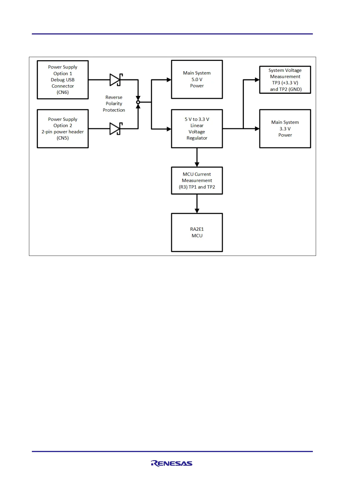
Figure 6. Power Supply Options
The MCU can be operated at a lower voltage than 3.3 V by removing the current measurement resistor and
powering the MCU via TP1.
Note: Other changes to the circuit where interfaces or pull-up resistors are used may also need to be
removed. Please review the schematic carefully before making these changes.
5.1.1.1 Option 1: Debug USB
5 V may be supplied from an external USB host to the USB debug connector (CN6) labelled POWER on the
board. Power from this source is connected to the main system 5 V power. Reverse current protection is
provided between this connector and the main system 5 V power.
5.1.1.2 Option 2: Header Connector CN5
5 V may be supplied from an external power supply to connector CN5. CN5 is a standard 2-pin header on a
0.1” (2.54 mm) pitch. Pin 1 is GND, and pin 2 is +5 V. Power from this source is connected to the main
system 5 V power. Reverse current protection is provided between CN5 and the main system 5 V power.
5.1.2 Power Supply Considerations
The on-board LDO regulator which supplies +3.3 V has a built-in current limit of 2.0 A. Make sure the total
current required by the RA MCU, any active on-board features, and any connected peripheral devices does
not exceed this limit.
Note: The total current available from a typical USB host is 100 mA before enumeration, and 500 mA
maximum. Depending on the configuration of the kit, multiple power sources may be required.
5.1.3 Power-up Behavior
When powered, the green LED marked POWER will illuminate.
 Loading...


