EasyManuals Logo

Renesas RA2 Series User Manual

Renesas RA2 Series
30 pages
To Next Page IconTo Next Page
To Previous Page IconTo Previous Page
Page #18 background imageLoading...
Page #18 background image
Renesas RA Family FPB-RA2E1 v1User's Manual
R20UT4956EG0100 Rev 1.00 Page 14 of 24
Jul.23.21
Table 6. JTAG/SWD/ETM Connector CN4
JTAG/SWD/ETM Connector
FPB-RA2E1
Pin
JTAG Pin Name
SWD Pin Name
ETM Pin Name
Signal/Bus
CN4-1
Vtref
Vtref
Vtref
+3V3
CN4-2
TMS
SWDIO
N/A
P108/SWDIO
CN4-3
GND
GND
GND
GND
CN4-4
TCK
SWCLK
N/A
P300/SWCLK
CN4-5
GND
GND
GND
GND
CN4-6
TDO
SWO
N/A
P109
CN4-7
Key
Key
Key
NC
CN4-8
TDI
NC/EXTb
N/A
P110
CN4-9
GNDDetect
GNDDetect
GNDDetect
GND
CN4-10
nSRST
nSRST
nSRST
RESET#
To configure the FPB-RA2E1 board to use the Debug In mode, configure the jumpers using the following
table.
Table 7. Debug In Mode Jumper Configuration
Location
Default Open/Closed
Function
CN1
Jumper on pins 2-3
E2 Emulator On-Board debugger held in reset
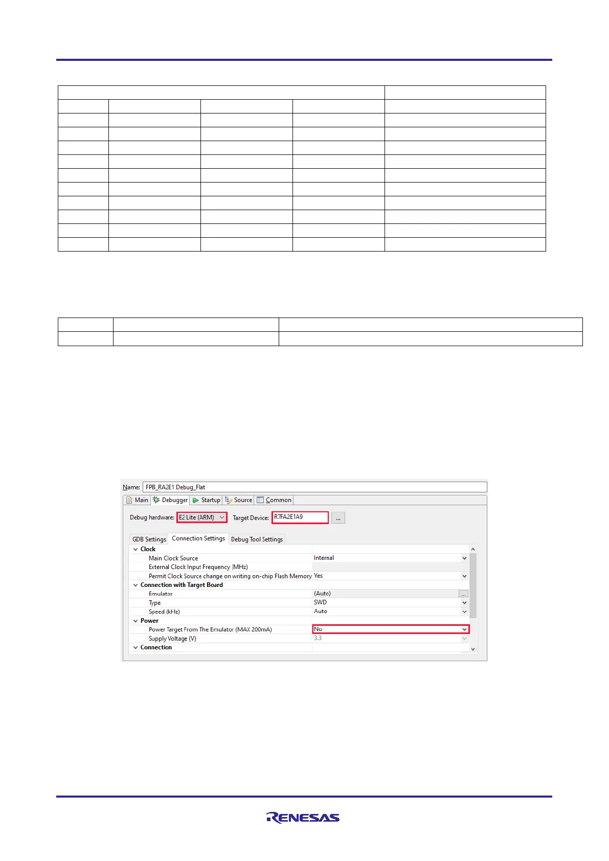
5.2.3 Debugger Settings in e
2
studio
Figure 8 shows the settings for e
2
studio when creating a new project for the FPB-RA4E1 Fast Prototyping
Board.
[Debug hardware]: Select [E2 Lite (ARM)]
[Power Target From The Emulator]: Select [No]
[Target Device]: Select [R7FA2E1A9]
Figure 8. e
2
Studio Debugger Settings

Table of Contents

Other manuals for Renesas RA2 Series

Questions and Answers:

Question and Answer IconNeed help?

Do you have a question about the Renesas RA2 Series and is the answer not in the manual?

Renesas RA2 Series Specifications

General IconGeneral
BrandRenesas
ModelRA2 Series
CategoryMotherboard
LanguageEnglish

Related product manuals