RC22312A/RC32312A Evaluation Board Manual
R31UH0022EU0100 Rev.1.00
Mar 28, 2023
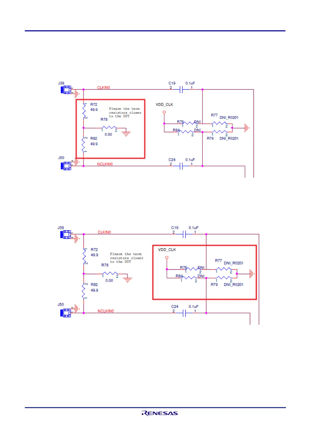
1.2.5. Clock Inputs
The RC32312A can accept four differential clock inputs to be used as a jitter attenuator source. To enable
proper connection, make sure the input termination resistor setup corresponds to the input signal that is
connected. The evaluation board default termination setup has 50Ω to GND at each leg.
Figure 14. Input Clock Termination Schematic
The RC32312A contains internal AC-coupling for LVDS, HCSL, LVCMOS signals. Supported frequency ranges
of the clock inputs are 1kHz to 1GHz in differential mode, and 1kHz to 250MHz in single-ended mode.
Pull-up and pull-down resistors apart of the CLKIN path can be used for common mode voltage adjustments.
Figure 15. Input Clock Pull-up/down Schematic
Note: Clock inputs are only used with RC32312A devices.
 Loading...


