RC22312A/RC32312A Evaluation Board Manual
R31UH0022EU0100 Rev.1.00
Mar 28, 2023
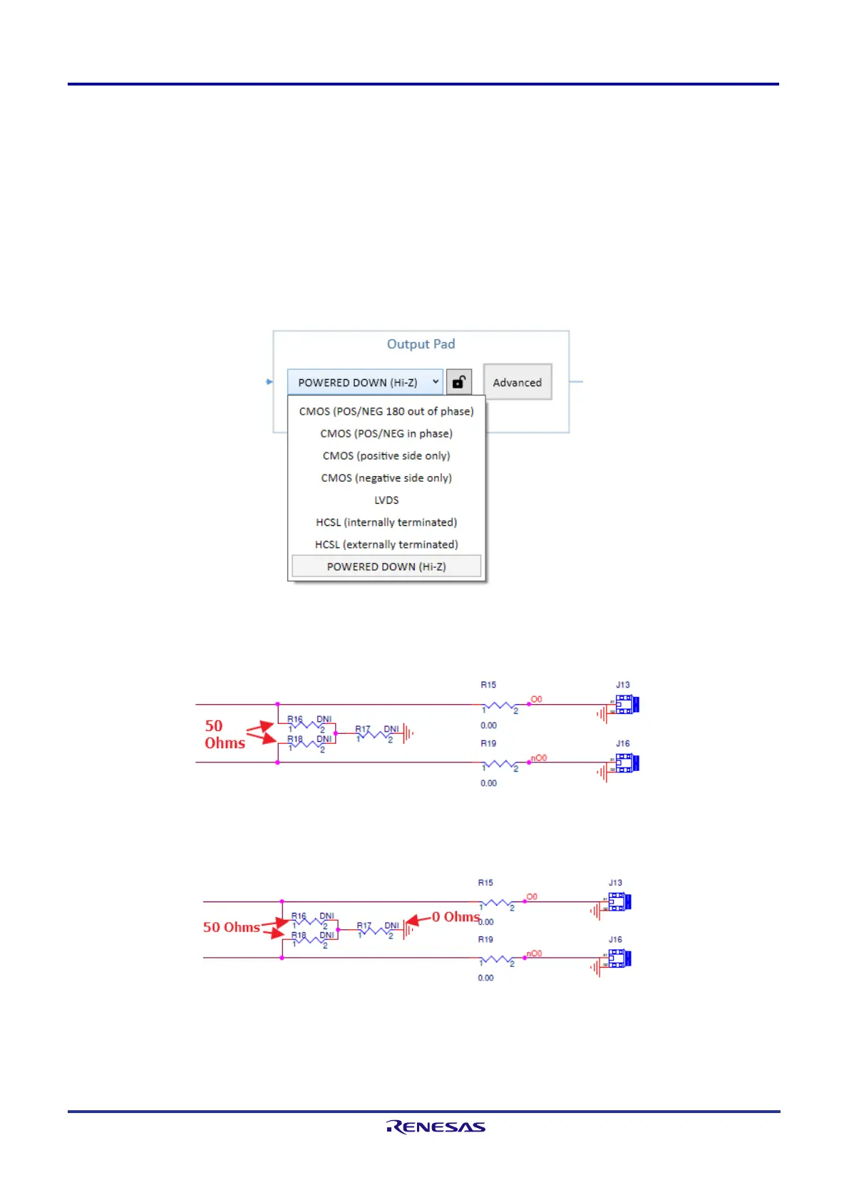
1.2.6. Clock Outputs
Each of the 12 differential output pairs can be programmed to LVDS, HCSL or CMOS logic type.
■
The HCSL mode supports HCSL by default and can be modified to support other modes by changing the
amplitude and enabling/disabling the internal termination.
■
For CMOS output type, output phase of each pin can be programmed to be 180 degrees out-of-phase, in-
phase, or single pin output.
■
LVDS outputs can be configured to 350mV or 400mV swing up to 1V common mode voltage.
■
Each output can also be tri-stated when not being used.
Output terminations on the evaluation board can be populated to support the different output types.
Figure 16. Output Type Options
Place 50Ω across each leg, for a total 100Ω across, to terminate for LVDS.
Figure 17. LVDS Input Clock Termination
Place 50Ω to GND at each leg for HCSL terminations.
Figure 18. HCSL Input Clock Termination
 Loading...


