RC22312A/RC32312A Evaluation Board Manual
R31UH0022EU0100 Rev.1.00
Mar 28, 2023
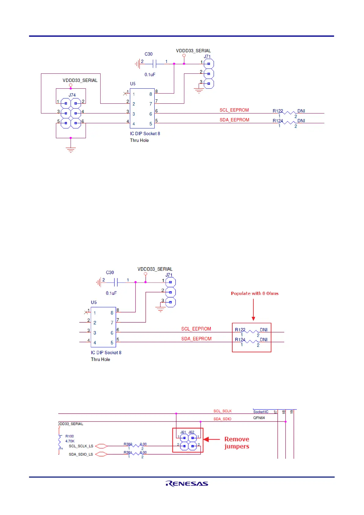
Figure 22. EEPROM Schematic
The A1 and A2 pins are the EEPROM address inputs that can be pull either high or low using jumpers at J74 to
define the device address. By default, jumpers can be removed so that A1 and A2 are left floating as they are
internally pulled down to GND in most EEPROM devices.
The WP pin is the write-protect input. When the WP pin is pulled down to GND (Low), the EEPROM can have
normal write operations. When it is pulled up directly to V
CC
(High), all write operations are inhibited. The WP pin
can be controlled with a jumper at J71.
To establish a connection to the EEPROM, the SDA and SCL traces must be connected to the FTDI
communication path. Populate R122 and R124 with 0 Ohms to make the connection. This will allow software
features like RICBox to communicate with the EEPROM device.
Figure 23. EEPROM Connection Resistors
When the device attempts to load an EEPROM configuration during start-up, the FTDI I
2
C controller can cause
interference. The FTDI device can be removed from the I
2
C trace path by removing jumpers J61 and J62. This
will also disconnect RICBox from communicating with the RC22312A/RC32312A device.
Figure 24. FTDI to I
2
C Communication Jumpers
 Loading...


