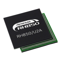
RH850/U2A 144pin 1. Overview
R20UT5089ED0101 Rev.1.01 Page 1 of 56
July 08, 2022
1.2 Supported Main Boards
This piggyback board can be used as a standalone board, or it can be mated with a main
board. The following main boards are supported:
• Y-RH850-X1X-MB-T1-V1
• Y-RH850-X1X-MB-T2-Vx
• Y-RH850-X2X-MB-T1-V1
1.3 Main Features
• Burn-in socket for mounting of the device
• Several power set-up options
− Combined operation with powering from main board
− Stand-alone operation with single power supply (e.g. 3.3 V or 5.0 V only)
− Stand-alone operation with flexible, individual power supply (typ. 1.12 V, 3.3 V, 5.0 V)
Refer to
3.3 Device Core Voltage (VDD) Selection
for further details about VDD
voltage.
• Debugging and programming interface:
− 14-pin LPD/JTAG Debug Connector (e.g. for using E2 OCD Emulator or PG-FP6 Flash
Programmer)
• Pin headers for direct access to each device pin
• Reset switch
• External clock circuit with an exchangeable 16/20/24/40 MHz Crystal Resonator
• General purpose signaling LEDs
• Jumpers for device mode selection and other configuration options
• Operating temperature from 0 °C to +40 °C

 Loading...