RL78/G13 CHAPTER 29 ELECTRICAL SPECIFICATIONS
R01UH0146EJ0100 Rev.1.00 1017
Sep 22, 2011
Caution The pins mounted depend on the product. Refer to 2.1.1 20-pin products to 2.1.14 128-pin products,
and 2.1.15 Pins for each product (pins other than port pins).
Notes 6. Use it with EV
DD0 ≥ Vb.
7. The smaller maximum transfer rate derived by using fMCK/6 or the following expression is the valid maximum
transfer rate.
Expression for calculating the transfer rate when 1.8 V ≤ EV
DD0 < 3.3 V and 1.6 V ≤ Vb ≤ 2.0 V
1
Maximum transfer rate =
[bps]
{−C
b × Rb × ln (1 −
1.5
Vb
)} × 3
1
Transfer rate × 2
− {−Cb × Rb × ln (1 −
1.5
Vb
)}
Baud rate error (theoretical value) =
× 100 [%]
(
1
Transfer rate
) × Number of transferred bits
* This value is the theoretical value of the relative difference between the transmission and reception sides.
8. This value as an example is calculated when the conditions described in the “Conditions” column are met.
Refer to Note 7 above to calculate the maximum transfer rate under conditions of the customer.
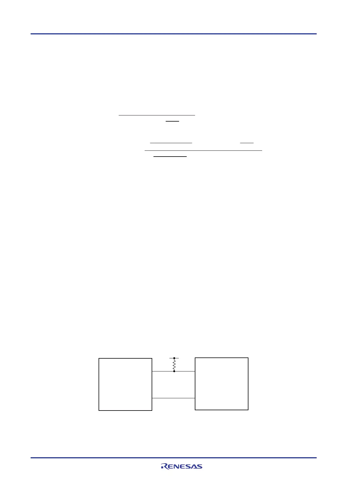
Caution Select the TTL input buffer for the RxDq pin and the N-ch open drain output (V
DD tolerance) mode for the
TxDq pin by using port input mode register g (PIMg) and port output mode register g (POMg).
Remarks 1. R
b[Ω]:Communication line (TxDq) pull-up resistance,
C
b[F]: Communication line (TxDq) load capacitance, Vb[V]: Communication line voltage
2. q: UART number (q = 0 to 3), g: PIM and POM number (g = 0, 1, 8, 14)
3. f
MCK: Serial array unit operation clock frequency
(Operation clock to be set by the CKSmn bit of serial mode register mn (SMRmn).
m: Unit number, n: Channel number (mn = 00 to 03, 10 to 13))
4. V
IH and VIL below are observation points for the AC characteristics of the serial array unit when
communicating at different potentials in UART mode.
4.0 V ≤ EV
DD0 ≤ 5.5 V, 2.7 V ≤ Vb ≤ 4.0 V: VIH = 2.2 V, VIL = 0.8 V
2.7 V ≤ EV
DD0 < 4.0 V, 2.3 V ≤ Vb ≤ 2.7 V: VIH = 2.0 V, VIL = 0.5 V
1.8 V ≤ EV
DD0 < 3.3 V, 1.6 V ≤ Vb ≤ 2.0 V: VIH = 1.5 V, VIL = 0.32 V
5. UART2 cannot communicate at different potential when bit 1 (PIOR1) of peripheral I/O redirection register
(PIOR) is 1.
UART mode connection diagram (during communication at different potential)
User's device
TxDq
RxDq
Rx
Tx
V
b
R
b
RL78/G13
<R>
<R>
<R>
<R>

 Loading...


