RL78/G13 CHAPTER 29 ELECTRICAL SPECIFICATIONS
R01UH0146EJ0100 Rev.1.00 1021
Sep 22, 2011
Caution The pins mounted depend on the product. Refer to 2.1.1 20-pin products to 2.1.14 128-pin products,
and 2.1.15 Pins for each product (pins other than port pins).
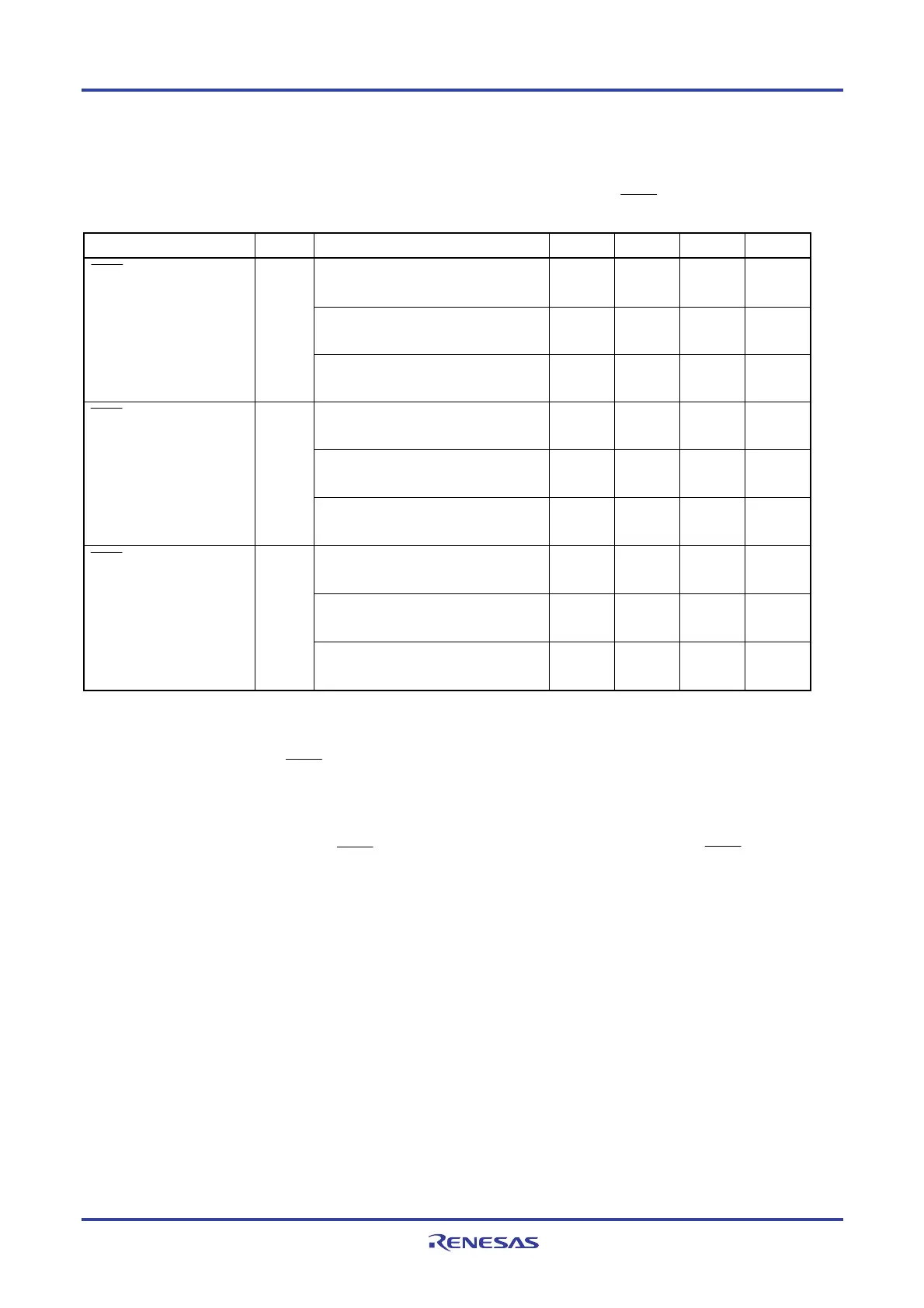
(8) Communication at different potential (2.5 V, 3 V) (f
MCK/4) (CSI mode) (master mode, SCKp... internal clock output) (1/2)
(TA = −40 to +85°C, 1.8 V ≤ EVDD0 = EVDD1 ≤ VDD ≤ 5.5 V, VSS = EVSS0 = EVSS1 = 0 V)
Parameter Symbol Conditions MIN. TYP. MAX. Unit
4.0 V ≤ EVDD0 ≤ 5.5 V, 2.7 V ≤ Vb ≤ 4.0 V,
C
b = 30 pF, Rb = 1.4 kΩ
300
Note
ns
2.7 V ≤ EVDD0 < 4.0 V, 2.3 V ≤ Vb ≤ 2.7 V,
C
b = 30 pF, Rb = 2.7 kΩ
500
Note
ns
SCKp cycle time tKCY1
1.8 V ≤ EV
DD0 < 3.3 V, 1.6 V ≤ Vb ≤ 2.0 V,
C
b = 30 pF, Rb = 5.5 kΩ
1150
Note
ns
4.0 V ≤ EVDD0 ≤ 5.5 V, 2.7 V ≤ Vb ≤ 4.0 V,
C
b = 30 pF, Rb = 1.4 kΩ
t
KCY1/2 − 75 ns
2.7 V ≤ EVDD0 < 4.0 V, 2.3 V ≤ Vb ≤ 2.7 V,
C
b = 30 pF, Rb = 2.7 kΩ
t
KCY1/2 −
170
ns
SCKp high-level width tKH1
1.8 V ≤ EV
DD0 < 3.3 V, 1.6 V ≤ Vb ≤ 2.0 V,
C
b = 30 pF, Rb = 5.5 kΩ
t
KCY1/2 −
458
ns
4.0 V ≤ EVDD0 ≤ 5.5 V, 2.7 V ≤ Vb ≤ 4.0 V,
C
b = 30 pF, Rb = 1.4 kΩ
t
KCY1/2 − 12 ns
2.7 V ≤ EVDD0 < 4.0 V, 2.3 V ≤ Vb ≤ 2.7 V,
C
b = 30 pF, Rb = 2.7 kΩ
t
KCY1/2 − 18 ns
SCKp low-level width tKL1
1.8 V ≤ EV
DD0 < 3.3 V, 1.6 V ≤ Vb ≤ 2.0 V,
C
b = 30 pF, Rb = 5.5 kΩ
t
KCY1/2 − 50 ns
Note The value must also be 4/fCLK or more.
Cautions 1. Select the TTL input buffer for the SIp pin and the N-ch open drain output (V
DD tolerance) mode for
the SOp pin and SCKp pin by using port input mode register g (PIMg) and port output mode register
g (POMg).
2. Use it with EV
DD0 ≥ Vb.
Remarks 1. R
b[Ω]:Communication line (SCKp, SOp) pull-up resistance, Cb[F]: Communication line (SCKp, SOp) load
capacitance, V
b[V]: Communication line voltage
2. p: CSI number (p = 00, 01, 10, 20, 30, 31), m: Unit number , n: Channel number (mn = 00, 01, 02, 10,
12, 13), g: PIM and POM number (g = 0, 1, 4, 5, 8, 14)
3. V
IH and VIL below are observation points for the AC characteristics of the serial array unit when
communicating at different potentials in CSI mode.
4.0 V ≤ EV
DD0 ≤ 5.5 V, 2.7 V ≤ Vb ≤ 4.0 V: VIH = 2.2 V, VIL = 0.8 V
2.7 V ≤ EV
DD0 < 4.0 V, 2.3 V ≤ Vb ≤ 2.7 V: VIH = 2.0 V, VIL = 0.5 V
1.8 V ≤ EVDD0 < 3.3 V, 1.6 V ≤ Vb ≤ 2.0 V: VIH = 1.5 V, VIL = 0.32 V
4. CSI01 of 48-, 52-, 64-pin products, and CSI11 and CSI21 cannot communicate at different potential. Use
other CSI for communication at different potential.
<R>
<R>
<R>
<R>

 Loading...


