RL78/G13 CHAPTER 2 PIN FUNCTIONS
R01UH0146EJ0100 Rev.1.00 95
Sep 22, 2011
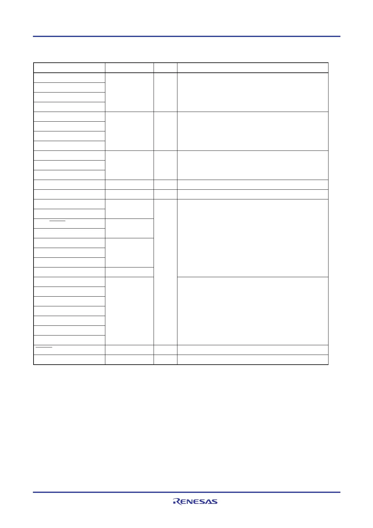
Table 2-3. Connection of Unused Pins (128-pin products) (4/4)
Pin Name I/O Circuit Type I/O Recommended Connection of Unused Pins
P115/ANI26
P116/ANI25
P117/ANI24
P120/ANI19
11-U I/O
Input: Independently connect to EV
DD0, EVDD1 or EVSS0, EVSS1
via a resistor.
Output: Leave open.
P121/X1
P122/X2/EXCLK
P123/XT1
P124/XT2/EXCLKS
37-C Input Independently connect to V
DD or VSS via a resistor.
P125
P126
P127
8-R I/O
Input: Independently connect to EV
DD0, EVDD1 or EVSS0, EVSS1
via a resistor.
Output: Leave open.
P130 3-C Output Leave open.
P137/INTP0 2 Input Independently connect to VDD or VSS via a resistor.
P140/PCLBUZ0/INTP6
P141/PCLBUZ1/INTP7
8-R
P142/SCK30/SCL30
P143/SI30/RxD3/SDA30
5-AN
P144/SO30/TxD3
P145/TI07/TO07
P146/(INTP4)
8-R
P147/ANI18 11-U
Input: Independently connect to EV
DD0, EVDD1 or EVSS0, EVSS1
via a resistor.
Output: Leave open.
P150/ANI8
P151/ANI9
P152/ANI10
P153/ANI11
P154/ANI12
P155/ANI13
P156/ANI14
11-G
I/O
Input: Independently connect to V
DD or VSS via a resistor.
Output: Leave open.
RESET 2 Input Connect directly or via a resistor to VDD.
REGC
− −
Connect to VSS via capacitor (0.47 to 1
μ
F).
Remarks 1. With products not provided with an EVDD0, EVDD1, EVSS0, or EVSS1 pin, replace EVDD0 and EVDD1 with VDD, or
replace EV
SS0 and EVSS1 with VSS.
2. Functions in parentheses in the above figure can be assigned via settings in the peripheral I/O redirection
register (PIOR).
<R>

 Loading...


