RL78/G13 CHAPTER 12 SERIAL ARRAY UNIT
R01UH0146EJ0100 Rev.1.00 553
Sep 22, 2011
(5) Higher 7 bits of the serial data register mn (SDRmn)
The SDRmn register is the transmit/receive data register (16 bits) of channel n. Bits 8 to 0 (lower 9 bits) of SDR00,
SDR01, SDR10
Note 1
, SDR11
Note 1
or bits 7 to 0 (lower 8 bits) of SDR02, SDR03, SDR10
Note 2
, SDR11
Note 2
, SDR12
and SDR13 function as a transmit/receive buffer register, and bits 15 to 9 are used as a register that sets the
division ratio of the operation clock (f
MCK).
If the CCSmn bit of serial mode register mn (SMRmn) is cleared to 0, the clock set by dividing the operating clock
by the higher 7 bits of the SDRmn register is used as the transfer clock.
The lower 8/9 bits of the SDRmn register function as a transmit/receive buffer register. During reception, the
parallel data converted by the shift register is stored in the lower 8/9 bits, and during transmission, the data to be
transmitted to the shift register is set to the lower 8/9 bits.
The SDRmn register can be read or written in 16-bit units.
However, the higher 7 bits can be written or read only when the operation is stopped (SEmn = 0). During operation
(SEmn = 1), a value is written only to the lower 8/9 bits of the SDRmn register. When the SDRmn register is read
during operation, 0 is always read.
Reset signal generation clears the SDRmn register to 0000H.
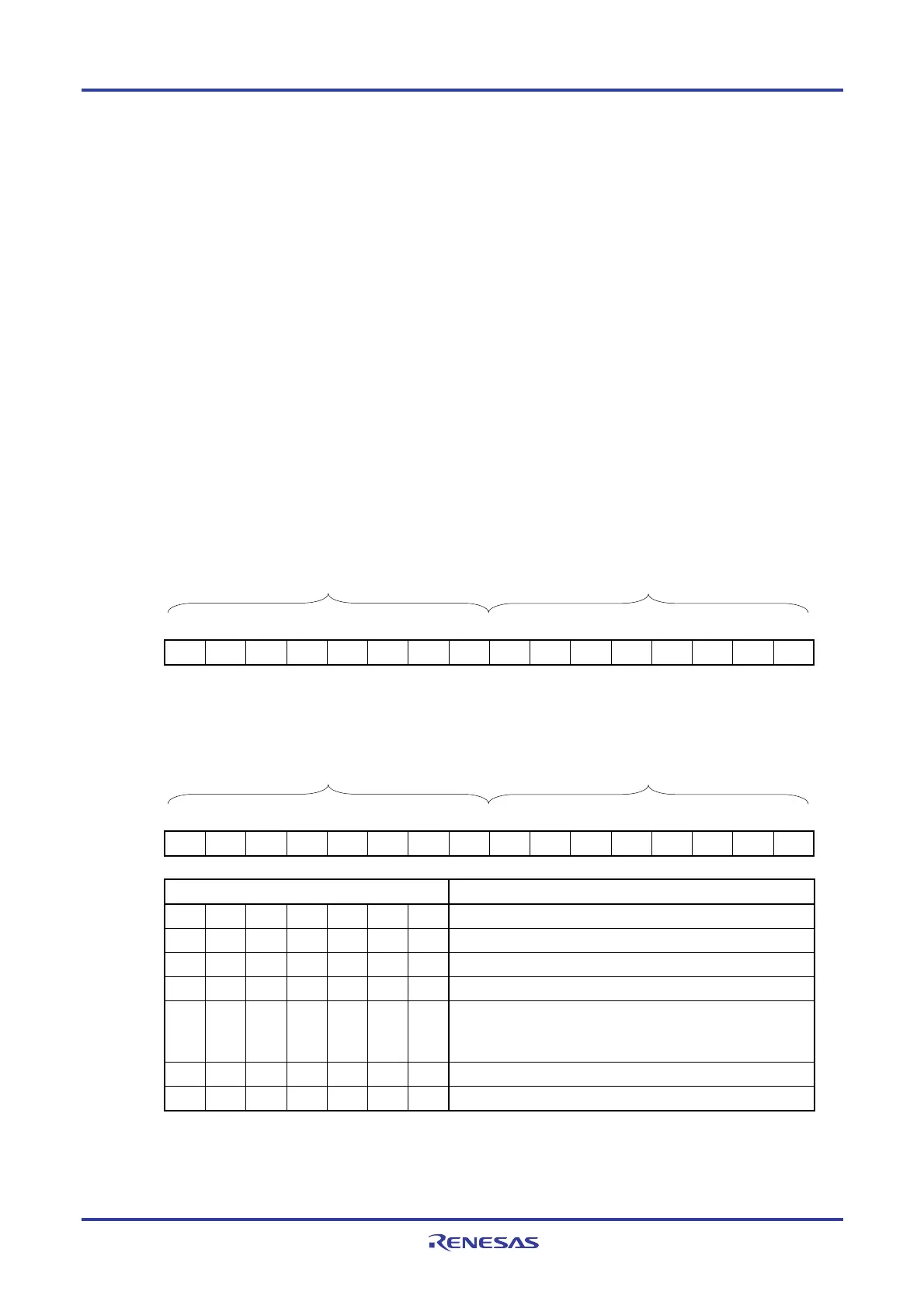
Figure 12-9. Format of Serial Data Register mn (SDRmn)
Address: FFF10H, FFF11H (SDR00), FFF12H, FFF13H (SDR01) After reset: 0000H R/W
FFF48H, FFF49H (SDR10)
Note 1
, FFF4AH, FFF4BH (SDR11)
Note 1
Symbol 15 14 13 12 11 10 9 8 7 6 5 4 3 2 1 0
SDRmn 0
Address: FFF44H, FFF45H (SDR02), FFF46H, FFF47H (SDR03), After reset: 0000H R/W
FFF48H, FFF49H (SDR10)
Note 2
, FFF4AH, FFF4BH (SDR11)
Note 2
FFF14H, FFF15H (SDR12), FFF16H, FFF17H (SDR13)
Symbol 15 14 13 12 11 10 9 8 7 6 5 4 3 2 1 0
SDRmn 0
SDRmn[15:9] Transfer clock setting by dividing the operating clock (fMCK)
0 0 0 0 0 0 0 fMCK/2
0 0 0 0 0 0 1 fMCK/4
0 0 0 0 0 1 0 fMCK/6
0 0 0 0 0 1 1 fMCK/8
•
•
•
•
•
•
•
•
•
•
•
•
•
•
•
•
•
•
•
•
•
•
•
•
1 1 1 1 1 1 0 fMCK/254
1 1 1 1 1 1 1 fMCK/256
Notes 1. 20, 100 and 128-pin products
2. 20 to 64-pin products
(Cautions and remarks are listed on the next page.)
FFF11H (SDR00)
FFF10H (SDR00)
FFF45H (SDR02)
FFF44H (SDR02)
<R>
<R>

 Loading...


