91
27DV-S100
27DV-CS10
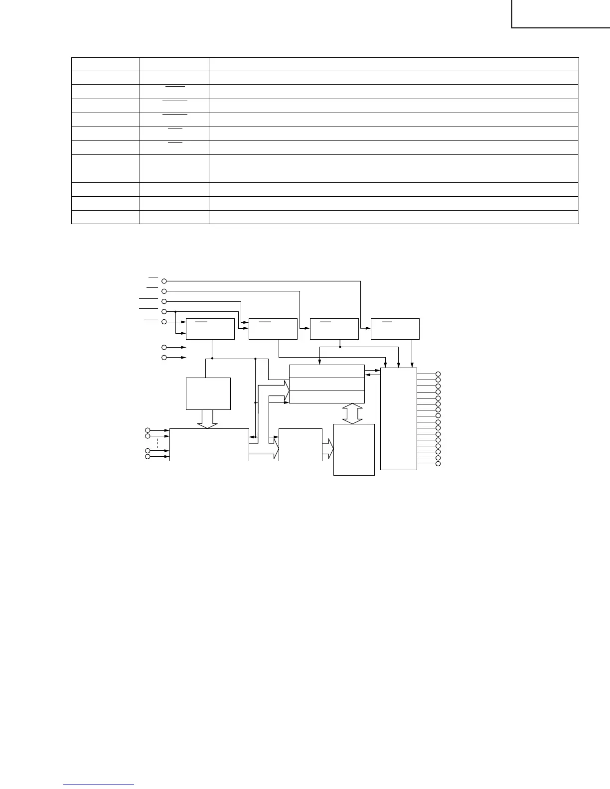
RAS clock
generator
CAS clock
generator
WE clock
generator
Data I/O Bus
Column decoders
Sense amplifiers
Refresh
counter
Address buffers
and predecoders
Row
decoders
Memory
array
OE clock
generator
I/O1
I/O2
I/O3
I/O4
I/O5
I/O6
I/O7
I/O8
I/O9
I/O10
I/O11
I/O12
I/O13
I/O14
I/O15
I/O16
I/O
Buffer
9
Y
0
-Y
8
X
0
-X
8
512
512 16
OE
WE
UCAS
LCAS
RAS
V
CC
V
SS
A0
A1
A7
A8
IC702 IX3420CE 4M EDO DRAM
Terminal Terminal name Function
16-19, 22-26 A0-A8 Address inputs.
14 RAS Row address strobe.
28 UCAS Column address strobe/upper byte control.
29 LCAS Column address strobe/lower byte control.
13 WE Write enable.
27 OE Output enable.
2-5, 7-10 DQ
1-DQ16 Data inputs/outputs.
31-34, 36-39
1, 6, 20 VCC +3.3V power supply.
21, 35, 40 VSS 0V ground.
11-12, 15, 30 NC No connection.
• Block Diagram