LC-32/40/46LE600E/RU/S (1st Edition)
6 – 13
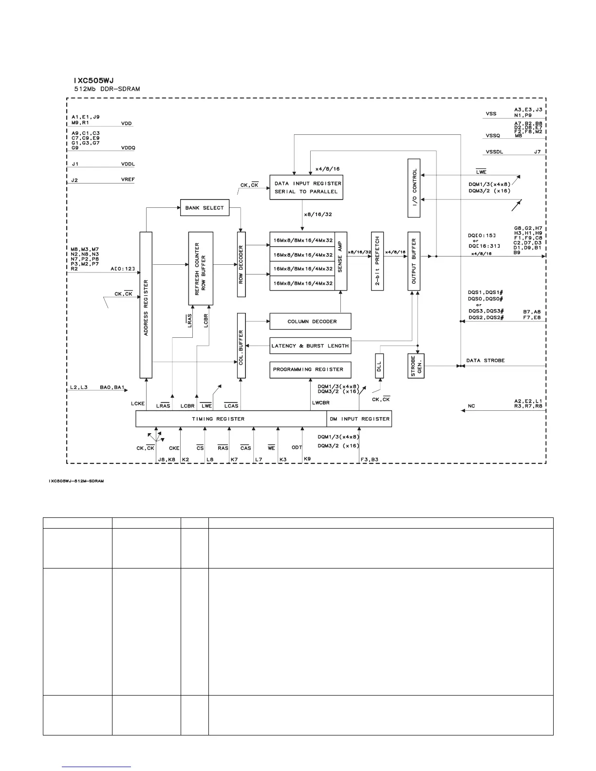
2.10. IC3501, IC3502 (RH-iXC505WJQZQ)
2.10.1 Block Diagram
2.10.2 Pin Connections and short description
Pin No. Pin Name I/O Pin Function
J8, K8 CK, CK# I Clock:
CK and CK# are differential clock inputs. All address and control input signals are sampled on the
crossing of the positive edge of CK and negative edge of CK#.
Output (read) data is referenced to the crossings of CK and CK# (both directions of crossing).
K2 CKE I Clock Enable:
CKE HIGH activates, and CKE Low deactivates, internal clock signals and device input buffers and
output drivers.
Taking CKE Low provides Pre charge Power-Down and Self Refresh operation (all bank idle), or
Active Power-Down (row Active in any bank).
CKE is synchronous for power down entry and exit, and for self refresh entry. CKE is asynchro-
nous for self refresh exit.
After VREF has become stable during the power on and initialization sequence, it must be main-
tained for proper operation of the CKE receiver. For proper self-refresh entry and exit, VREF must
be maintained to this input.
CKE must be maintained high throughout read and write accesses. Input buffers, excluding CK,
CK#, ODT and CKE are disabled during power-down. Input buffers, excluding CKE are disabled
during self refresh.
L8 CS# I Chip Select:
All commands are masked when CS# is registered HIGH.
CS# provides for external bank selection on systems with multiple banks.
CS# is considered part of the command code.