LC-32/40/46LE600E/RU/S (1st Edition)
6 – 3
2. Detailed ICs Information
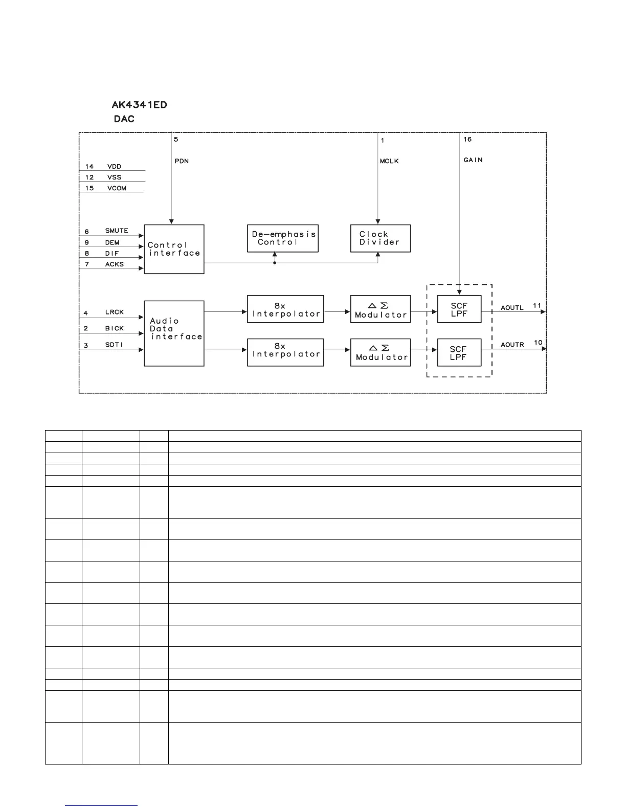
2.1. IC1301 (VHiAK4341ED-1Y)
2.1.1 Block Diagram
2.1.2 Pin Connections and short description
Pin No. Pin Name I/O Pin Function
1 MCLK I Master clock input pin. An external TTL clock should be input on this pin.
2 BICK I Audio serial data clock pin.
3 SDTI I Audio serial data input pin.
4 LRCK I L/R clock pin.
5 RDN I Power-down mode pin.
When at “L”, the AK4341 is in the power-down mode, held in reset and AOUTL/R are held in VCOM.
The AK4341 must be reset once upon power-up.
6 SMUTE I Soft mute pin in parallel control mode.
“H”: Enable, “L”: Disable
7 ACKS I Auto setting mode pin.
“L”: Manual setting mode, “H”: Auto setting mode.
8 DIF I Audio data interface format pin.
“L”: 24bit MSB justified, “H”; I2S.
9 DEM I De-emphasis enable pin.
“H”: Enable, “L”: Disable
10 AOUTR O Rch analog output pin.
When PDN pin = “L”, outputs VCOM voltage.
11 AOUTL O Lch analog output pin.
When PDN pin = “L”, outputs VCOM voltage.
12 HVDD I Output buffer power supply pin.
Normally connected to VSS with a 0.1µF ceramic capacitor in parallel with a 10µF electrolytic cap.
13 VSS — Ground pin.
14 VDD — DAC power supply pin.
15 VCOM O DAC common voltage pin.
Normally connected to VSS with a 10µF electrolytic cap.
Outputs VCOM VDD voltage either PDN pin = “L” or “H”.
16 GAIN I Gain control pin.
“H”: +6dB, “L”: 0dB, open: +12dB.
When PDN = “H”, the gain pin is connected to VDD and VSS with 50kΩ resister and held to VDD/2 when open.
When PDN = “L”, connected to VSS with 50kΩ resister.