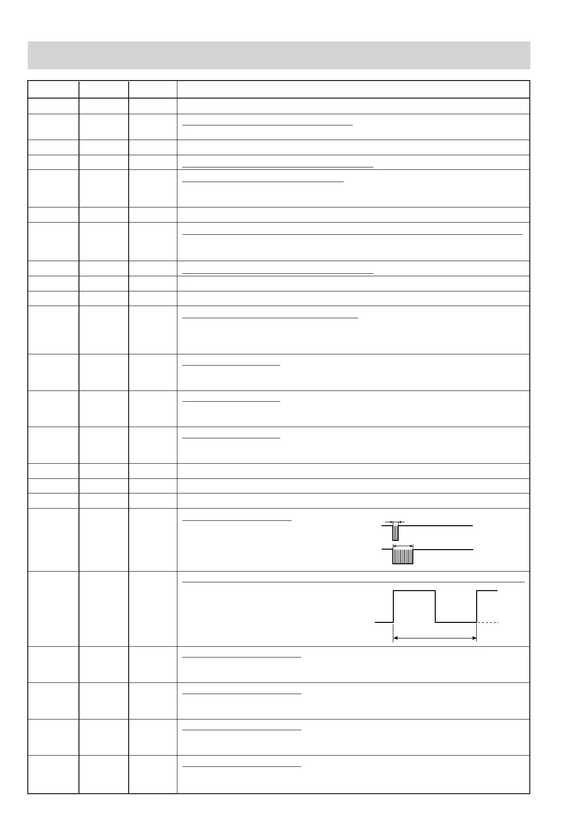
R-775(W)R-785(AL) - 22
1C1INTerminal not used.
2 VL1 IN Power source voltage input terminal.
Standard voltage for LCD.
3 AN7 IN Terminal to change the ON timing of the cook relay (RY2).
4-5 AN6-AN5 IN Heating constant compensation terminal.
6 AN4 IN
Signal coming from potentiometer.
By inputting DC voltage corresponding to the cooking mode set by the potentiometer,
this input is converted into the cooking mode by the A/D converter built into the LSI.
7 AN3 IN Terminal not used.
8 AN2 IN Input signal which communicates the door open/close information to LSI.
Door closed; “H” level signal.
Door opened; “L” level signal.
9 AN1 IN Heating constant compensation terminal.
10 AN0 IN Terminal to change functions to the Models.
11-14 P57-P54 OUT Terminal not used.
15 P53 IN Signal coming from touch tact switch.
When any one of J-8 line tact switches on jog switch unit matrix is touched, a
corresponding signal from P40, P41, P76 and P77 will be input into P53. When no
tact switch is touched, the signal is held at “L” level.
16 P52 IN Signal similar to P53.
When any one of J-7 line tact switches on key and jog switch unit matrix is touched,
a corresponding signal will be input into P52.
17 P51 IN Signal similar to P53.
When any one of J-4 line tact switches on key and jog switch unit matrix is touched,
a corresponding signal will be input into P51.
18 P50 IN Signal similar to P53.
When any one of J-3 line tact switches on key and jog switch unit matrix is touched,
a corresponding signal will be input into P50.
19 P47 OUT Memory (EEPROM) clock out.
20 P46 IN/OUT Memory (EEPROM) data input/output.
21-22 P45-P44 IN/OUT Terminal not used.
23 TOUT OUT Signal to sound buzzer.
A:Tact switch touch sound.
B: Completion sound.
24 INT2 IN Signal to synchronized LSI with commercial power source frequency(50Hz).
This is basic timing for time processing
of LSI.
25 P41 OUT Tact switch strobe signal.
Signal applied to tact switch section. A pulse signal is input to P51-P53 terminal
while one of J-6 line tact switches on matrix is touched.
26 P40 OUT Tact switch strobe signal.
Signal applied to tact switch section. A pulse signal is input to P51-P53 terminal
while one of J-5 line tact switches on matrix is touched.
27 P77 OUT Tact switch strobe signal.
Signal applied to tact switch section. A pulse signal is input to P50-P53 terminal
while one of J-2 line tact switches on matrix is touched.
28 P76 OUT Tact switch strobe signal.
Signal applied to tact switch section. A pulse signal is input to P50-P53 terminal
while one of J-1 line tact switches on matrix is touched.
The I/O signal of the LSI are detailed in the following table.
Pin No. Signal I/O Description
20 msec.
H : GND
L (-5V)
DESCRIPTION OF LSI