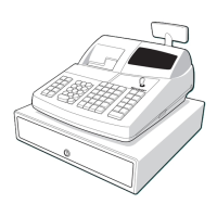
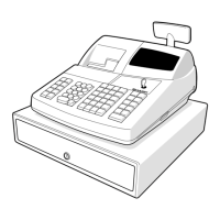
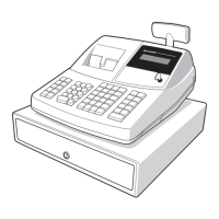
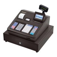
XE-A40S
4 – 5
3. KEYSCAN MATRIX
4. DISPLAY
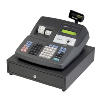
The XE-A40S has an LCD display, 5 x 7 dots, 2 lines, at the front side
and a 7-digit LED at the pop-up side.
• Display DIGIT signal
The above ST0 ~ ST6 are display digit signals.
ST0: 1st digit ~ ST6: 7th digit
• Display SEGMENT signal
The LED segment signal is outputted by writing SEGMENT data in
the /CS3 space.
Correspondence of DATA ~ SEGMENT
D0 ~ D6 → A ~ g
D7 → DP
[6] POWER SUPPLY
[7] RE-WRITING FLASH MEMORY
[8] DRAWER
The XE-A40S has a 1 drawer port. (No open sensor is provided.)
The driving time for the DRAWER solenoid are as follows: 50ms (max)
45ms (min)
[9] PRINT RATE
384 dots/1 line
[10] A/D CONVERSION
The printer power supply voltage should be measured at more than 10
ms after the printer is turned ON.
[11] BUZZER
PIEZO type BUZZER
The oscillating frequency is 4.0kHz ± 0.5kHz
[12] USB I/F
The XE-A40S is equipped with 1 USB port (slave) as a standard provi-
sion. By use of the USB general-purpose ASSP device M66291
(RENESAS), it sends and receives USB data. The M66291 is mapped
to the /CS1 area (28000H ~ 3FFFFFH). The CPU and the M66291 are
connected as shown in the figure below.
<CPU Port>
Access from CPU to M66291 : 28000H + Register Address (00~77H)
Input clock uses 24MHz.
[13] RESET
The RESET signal is generated when:
1) The mode key switch is turned from SRV to a position other than
SRV'(excluding OFF).
2) The power is turned ON more than 10 seconds after the power is
turned OFF. (The reset signal may not be issued if the POWER-
OFF time is short.)
3) The mode key switch is turned from OFF to a position other than
OF (excluding the SRV position). (If the power-off time is less than
5 seconds, the reset signal may not be issued.)
CPUSTOST1ST2ST3ST4ST5ST6ST7ST8ST9
MODE P90 SRV PGM Time REG MGR X1/Z1 X2/Z2
Others P91 PF-R PF-J RPE HEAD UP JPE DRAWER
OPEN
MRS RS/CI
IPL from EP-ROM: After IPL Short pin is set to VCC position the
program is started from EP-ROM by turning on
the power.
The program on EP-ROM is transferred to flash
ROM by switching the banks through S-RAM.
FRONT:
POP UP:
VLED
VCC 5.0V
VDD 5.0V
24V
BATTERY
TRANS.
LM2574 +
power failure occurs..
PQ1CG2032
ON/OFF CONTROL
(MODE SW)
/POFF detection point
Measures should be taken to restore within 10 ms after a
Pin
No.
CPU PORT SIGNAL Application
19 P83 (INT1) /DREQUSE USB DMA CHANNEL 0 DMA
Request signal
18 P84 (INT2) /INTUSB USB Interrupt 0 Request signal
26 P74 /USBRST USB reset signal
CPU M66291
Vcc
A0
A1~A6
D0~D7
CS1
RD
WRL
WRH
INT2
INT1
/USBRST
5V
7
8
1.0{F
27Ω
27Ω
1.5kΩ
3.3V
1
3
2
4
USB Connector
Vbus
D+
D-
GND
IOVcc
D15/AD0
AD1~AD6
D0~D7
CS
RD
LWR
HWR/BYTE
INT0
Dreq0
Xin
Xout
24MHz
D+
D-
CoreVcc
Vbus
TrON