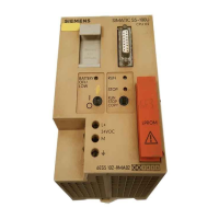
1.
Description
Principle of operation
AI! aspects of data exchange are initiated by the master PC.
The interface modules are addressed sequentially by the master PC
for
T
=
24
ms each. When the address is placed on the bus, the first
eight signals (low byte) are transferred immediately, and the second
eight signals (high byte) after
T/2
=
12 ms, and buffered on the
interface module or recalled from the buffer.
Seen
frorn the S5-010
PC,
the interface module is a module with
l6
inputs and
16
outputs. Fig. 11 shows the interaction between the
master PC and an S5-010
PC
by means of a block diagram.
Minimum times rnust be adhered to for the transmission mode (see
Fig. 12). Since the signals are transmitted through normal
I/O
modules as
24
V
signals, allowance must be made for the delay
times of the input module
(S5-150) and interface module, which are
necessary for
reasoi?s of noise immunity.
A
rr~inirnum time of
12
ms is necessary for transmitting eight signal
statuses in both directions. This gives a minimum time of
360
ms for
16
signal statuses (low and high bytes) to each of 15 PCs.
Interrupt processing
The interface module nas been equipped with
an
interrupt circuit in
order to improve the data throughput. The interrupt is generated
when the
S5-010 receives the output data frorn the master PC.
Cyclic execution
of the
STEP
5
program of the 55-010 controlier is
interrupted and the processor returns to the beginning
of the
program.
The first statements of the STEP 5 program are used for interrupt
processing, which needs a time of
T,
=
n
X
20 ps. After time
TB
+
tK
+
t,,
(t,:
input delay of interface module;
to:
delay due to bus
cable), the
S5-010 PC Ihas processed the input data (low byte
address
6.E-6.7)
of the master PC and updated its output data
affecting
interr~~pt processing (see
Fig.
13).
Certain output data (address
7.0..
7.7)
are enabled for the master
PC after
the change from low
10
high byte and can be processed
once rhe data are received by the
master PC
(TE:
input delay of
master PC).
Interrupt processing therelore ensures that
the transmission of data
from the master PC to the
S5-010 and from the SF?-010 to the
master
PC
takes place within the low byte and high byte, respec-
tively, of the same addressing interval
T.
interrupt processing is activated by closing two DIPFIX switches
I-._.1
L
A
Fig.
l?
Block diagram oi the kterface module
I
Data read
by
idterface module
1
1
!
Fig.
12
1-iming
of
tile transfer mode
High byte
I
Low byte
!
1
Address
601
.
.
.
E.7
I
Address
7@
...
7.7
1
l
I
1
Data
trar~sfer
l
Data output Interrupt genera- Upda:ed outp~t
l
Address output !ion
data
available Data transier
-..+
l
 Loading...