3
EN
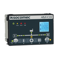
ATySController C35 - 549781A - SOCOMEC
11.4. Inputs ........................................................................26
11.4.1. Programmable Inhibit input ...................................................26
11.4.2. Position inputs ............................................................26
11.4.3. Fire input .................................................................26
11.4.4. RS485 ..................................................................26
12. PROGRAMMING ...................................................................27
12.1. Access to programming mode .....................................................27
12.2. Programing Menu Architecture .....................................................28
12.3. Input/output functions ............................................................30
12.4. Communication parameters .......................................................30
13. CHARACTERISTICS ................................................................31
14. PREVENTIVE MAINTENANCE ........................................................31
15. TROUBLE SHOOTING GUIDE ........................................................32
15.1. List of Faults ...................................................................32
16. ASSOCIATED PRODUCTS ...........................................................33
16.1. RTSE ........................................................................33
Annex I - 1. HMI Reminder .............................................................35
Annex I - 2. LED Functioning modes .....................................................36
Annex I - 3. Connection diagrams .......................................................37
Annexe I - 3.1. Connections with ATyS S ..............................................37
Annexe I - 3.2. Connections with ATyS dM .............................................38
Annexe I - 3.3. Connections with standard CC type based TSE .............................39
Annexe I - 3.4. Connections with standard CB type based TSE .............................40
Annex I - 4. Phase rotation check .......................................................41
Annex I - 5. Voltage/Frequency Levels configuration .........................................41
Annex I - 6. Timers ...................................................................42
Annexe I - 6.1. Fail timers and Return timers ...........................................42
Annexe I - 6.2. Cooldown and start gen delay timers .....................................42
Annexe I - 6.3. Dead band timer ODT .................................................42
Annexe I - 6.4. All timers’ chronograms ...............................................42
Annex I - 7. Priority settings & Retransfer ..................................................43
Annex I - 8. Tests ....................................................................43
Annex I - 9. C35 DPS Operating sequences ...............................................44
Annex I - 10. C35 standard operating sequence ............................................45
ANNEX II. MODBUS COMMUNICATION ADDRESS AND DESIGNATION DETAILS ..................48
Annex II - 1. Input / Output state ........................................................48
Annex II - 2. Status ..................................................................49
Annex II - 3. Voltage sensing ...........................................................50
Annex II - 4. Communication parameters ..................................................50
Annex II - 5. Maintenance .............................................................51
Annex II - 6. Product configuration .......................................................52