24
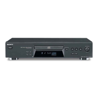
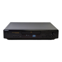
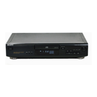
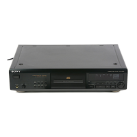
CDP-XE270/XE370
•
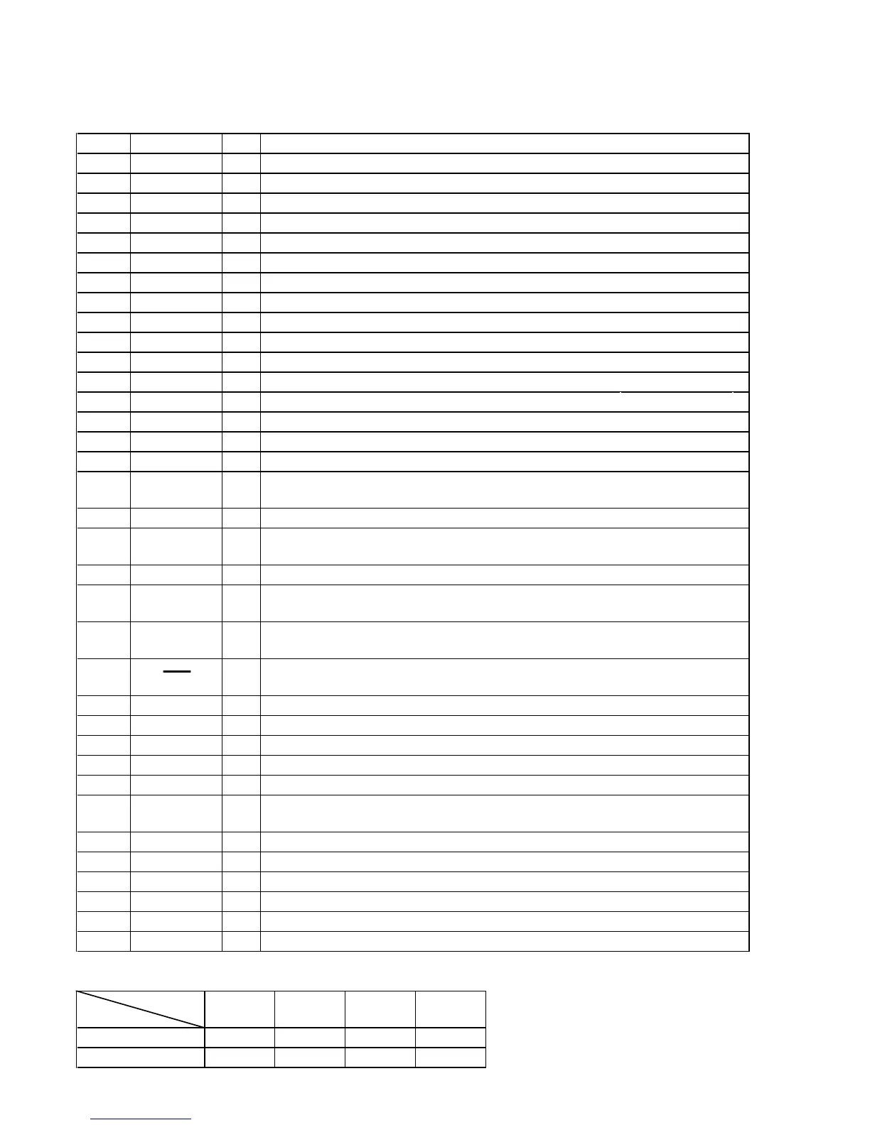
Pin No. Pin Name I/O Description
1
NC I Connected to the ground
2 RMIN I Remote control signal input from the remote control receiver (IC561)
3
NC I Connected to the ground
4 to 6
NC O Not used (open)
7
LDON/RW/OFF O CD-ROM/RW selection signal output “L”: CD-ROM, “H”: CD-RW
8 CLK O Serial data transfer clock signal output to the CXD2587Q (IC101)
9 SENS I Internal status (SENSE) signal input from the CXD2587Q (IC101)
10 DATA O Serial data output to the CXD2587Q (IC101)
11 SQCK O Subcode Q data reading clock signal output to the CXD2587Q (IC101)
12 SQSO I Subcode Q data signal input from the CXD2587Q (IC101)
13, 14
NC O Not used (open)
15 XLAT O Serial data latch pulse signal output to the CXD2587Q (IC101)
16 to 19
NC O Not used (open)
20 LDOUT O Loading motor (M151) drive signal output to the BA6956AN (IC631) “H” active *1
21 LDIN O Loading motor (M151) drive signal output to the BA6956AN (IC631) “H” active *1
22, 23 NC O Not used (open)
24 KEY0 I
Key input terminal (A/D input)
S501 to S504 (TIME, PLAY MODE, CLEAR, REPEAT) keys input
25 KEY1 I Key input terminal (A/D input) S520 (1/2) (l AMS L) keys input
26 KEY2 I
Key input terminal (A/D input) S520 (2/2) to S524, S526, S527
(l AMS L PUSH ENTER, A OPEN/CLOSE, H, X, x, M, m) keys input
27 NC O Not used (open)
28
ADJ/AFADJ/BD
TEST
I
Setting terminal for the test mode
“L”: ADJ test mode, “M”: AFADJ test mode, “H”: BD test mode
29 IN/OUT SW I
Loading in detect switch (S152) and loading out detect switch (S151) input terminal
“L”: load in, “H”: load out
30
RST I
System reset signal input from the reset signal generator (IC603) “L”: reset
For several hundreds msec. after the power supply rises, “L” is input, then it changes to “H”
31
EXTAL I Main system clock input terminal (4 MHz)
32
XTAL O Main system clock output terminal (4 MHz)
33
VSS — Ground terminal
34 to 41 NC O Not used (open)
42 to 47 S6 to S1 O
Segment drive signal output to the fluorescent indicator tube (FL501)
48 to 55
S7, S11, S12, S8,
S21, S10, S9, S20
O
Segment drive signal output to the fluorescent indicator tube (FL501)
56 to 62 S13 to S19 O
Segment drive signal output to the fluorescent indicator tube (FL501)
63 to 67 7G to 3G O
Grid drive signal output to the fluorescent indicator tube (FL501)
68 NC O Not used (open)
69, 70 2G, 1G O
Grid drive signal output to the fluorescent indicator tube (FL501)
71 VFDP (–30V)
— Power supply terminal (–30V) (for fluorescent indicator tube drive)
72 VDD (+5V) — Power supply terminal (+5V)
DISPLAY BOARD IC501 CXP82324-093Q
(SYSTEM CONTROLLER, FLUORESCENT INDICATOR TUBE DRIVER, KEY CONTROL)
*1 Loading motor (M151) control
OFF OUT IN BRAKE
LDIN (pin wa)
“L”“L”“H”“H”
LDOUT (pin w;)
“L”“H”“L”“H”
Operatio