– 12 –
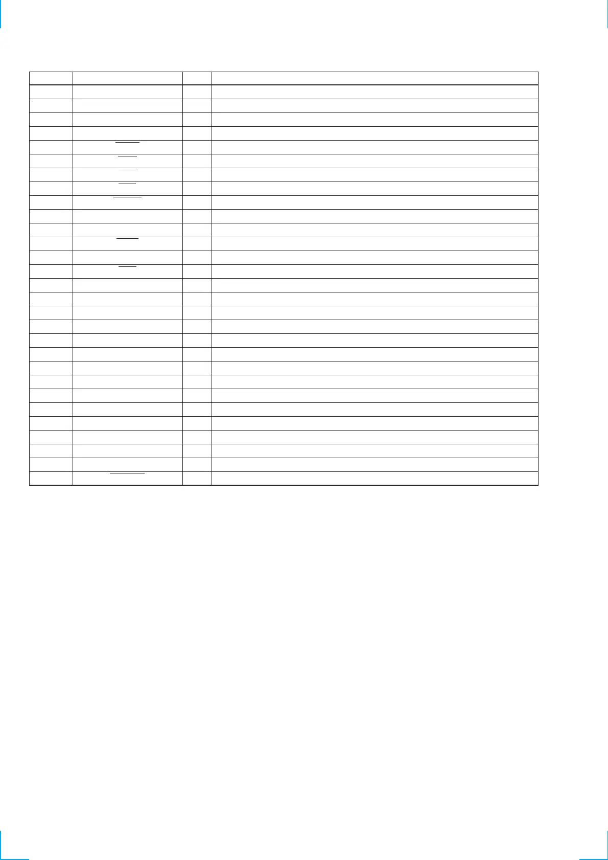
Pin No. Pin Name I/O Pin Description
52 PLLCKO O PLL clock output
53 PLLSI I PLL data input
54 AMON O AM ON output
55 — — Not used in this set.
56 FMST I/O ST-IND indication input/Forced Monaural output
57 SW4 I Switch 4 input (“L” active)
58 SW3 I Switch 3 input (“L” active)
59 SW1 I Switch 1 input (“L” active)
60 RESET I System reset input
61 SIRCS I Not used in this set.
62 KEYACK I Key input acknowledge
63 BUIN I Backup power supply detection input
64 BLKCK I Sub code • block • clock signal input (interruption)
65 SW2 I Switch 2 input (“L” active)
66 FCLK I Latch input for error correction result read-in. (interruption)
67 VSS0 — Ground
68 VDD1 — Power supply pin (+5 V)
69 X2 — Main system clock output (5 MHz)
70 X1 — Main system clock input (5 MHz)
71 VPP — Internal connection
72 XT2 — Sub system clock output (32.768 kHz)
73 XT1 — Sub system clock input (32.768 kHz)
74 VDD0 — Power supply pin (+5 V)
75 AVREF0 — Analog reference voltage input
76 KEYIN0 I Key input 0
77 KEYIN1 I Key input 1
78 S-METER I AM/FM S-meter voltage detection input
79 SD-IN I Signal detector input
80 LCDINH O LCD blank indication control output