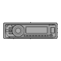
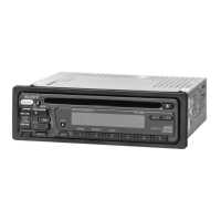
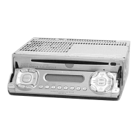
CDX-1150
– 19 – – 20 –
3-4. SCHEMATIC DIAGRAM — MAIN SECTION (1/3) — • Refer to page 29 for IC Block Diagrams.
(Page 21)
(Page 23)
• Waveforms (MODE:PLAY)
3
1
2
Approx. 600mVp-p
IC102
@£
(FE)
0V
IC102
9
(ARF)
1.3Vp-p
Approx. 200mVp-p
IC102
@™
(TE)
0V
Note:
• All capacitors are in µF unless otherwise noted. pF: µµF
50 WV or less are not indicated except for electrolytics
and tantalums.
• All resistors are in Ω and
1
/
4
W or less unless otherwise
specified.
•
¢
: internal component.
• C : panel designation.
• U : B+ Line.
• Power voltage is dc 14.4V and fed with regulated dc power
supply from ACC and BATT cords.
• Voltage and waveforms are dc with respect to ground
under no-signal conditions.
no mark : CD PLAY
• Voltages are taken with a VOM (Input impedance 10 MΩ).
Voltage variations may be noted due to normal produc-
tion tolerances.
• Waveforms are taken with a oscilloscope.
Voltage variations may be noted due to normal produc-
tion tolerances.
• Circled numbers refer to waveforms.
• Signal path.
J : CD
Note: The components identified by mark ! or dotted line
with mark ! are critical for safety.
Replace only with part number specified.
RTV servis Horvat
Kešinci, 31402 Semeljci
031-856-139
031-856-637
098-788-319
rtv-servis-horvat@os.tel.hr
Croatia