– 21 – – 22 –
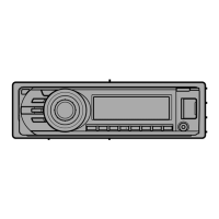
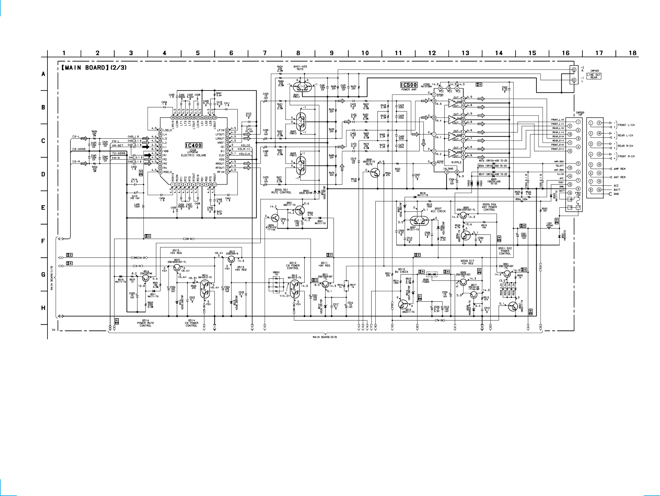
CDX-1150
Note:
• All capacitors are in µF unless otherwise noted. pF: µµF
50 WV or less are not indicated except for electrolytics
and tantalums.
• All resistors are in Ω and
1
/
4
W or less unless otherwise
specified.
• % : indicates tolerance.
• C : panel designation.
• U : B+ Line.
• Power voltage is dc 14.4V and fed with regulated dc power
supply from ACC and BATT cords.
• Voltage is dc with respect to ground under no-signal
(detuned) condition.
no mark : FM
< > : CD PLAY
• Voltages are taken with a VOM (Input impedance 10 MΩ).
Voltage variations may be noted due to normal produc-
tion tolerances.
• Signal path.
F : FM
f : AM
J : CD
3-5. SCHEMATIC DIAGRAM — MAIN SECTION (2/3) — • Refer to page 30 for IC Block Diagrams.
(Page 24)
(Page 20)