4-35
DSC-P72
COVER
COVER
4-3. PRINTED WIRING BOARDS
4-3. PRINTED WIRING BOARDS
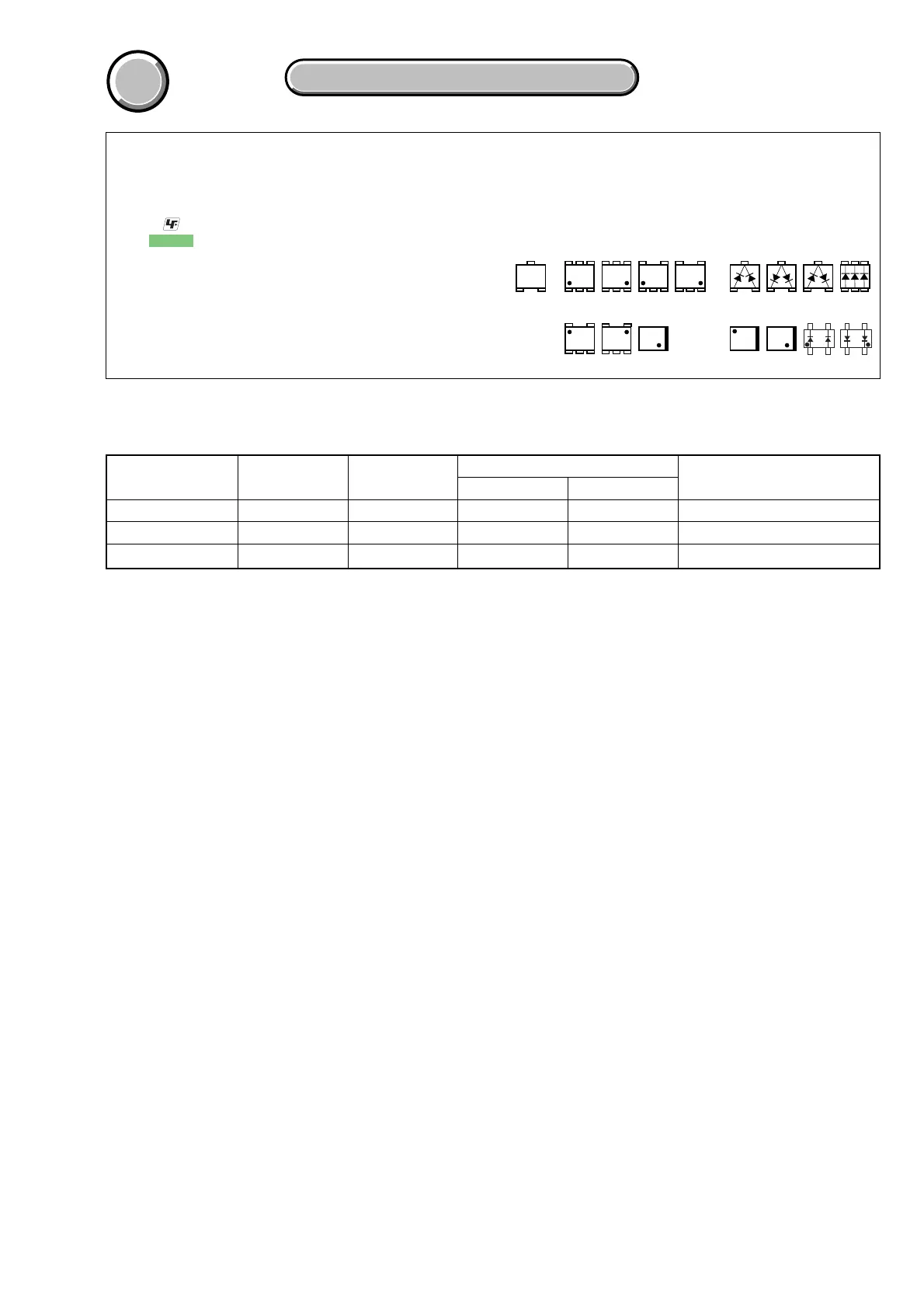
(For printed wiring boards)
• : Uses unleaded solder.
• : Pattern from the side which enables seeing.
(The other layers’ patterns are not indicated)
• Through hole is omitted.
• Circled numbers refer to waveforms.
• There are a few cases that the part printed on diagram
isn’t mounted in this model.
• C: panel designation
THIS NOTE IS COMMON FOR WIRING BOARDS
(In addition to this, the necessary note is printed in each block)
21
3
21
3
21
3
345
21
123
654
EB
C
31
5
5
2
46
123
54
43
12
12
43
312
45
534
12
34
21
12
43
46
2
5
31
12
4
3
• Chip parts.
Transistor Diode
board name
ST-82
JK BLOCK
SY-85
parts location
(shown on page)
4-47
–
4-48
waveform
(shown on page)
–
–
4-45
number of layers
4
1
8
layers not shown
2 to 3
–
2 to 7
CSP IC
–
–
IC151, 401, 501, 001, 301, 901
pattern
BOARD INFORMATION