HCD-DJ2i
65
USB BOARD IC901 TMP92CD28AFG-7AC9 (USB CONTROL)
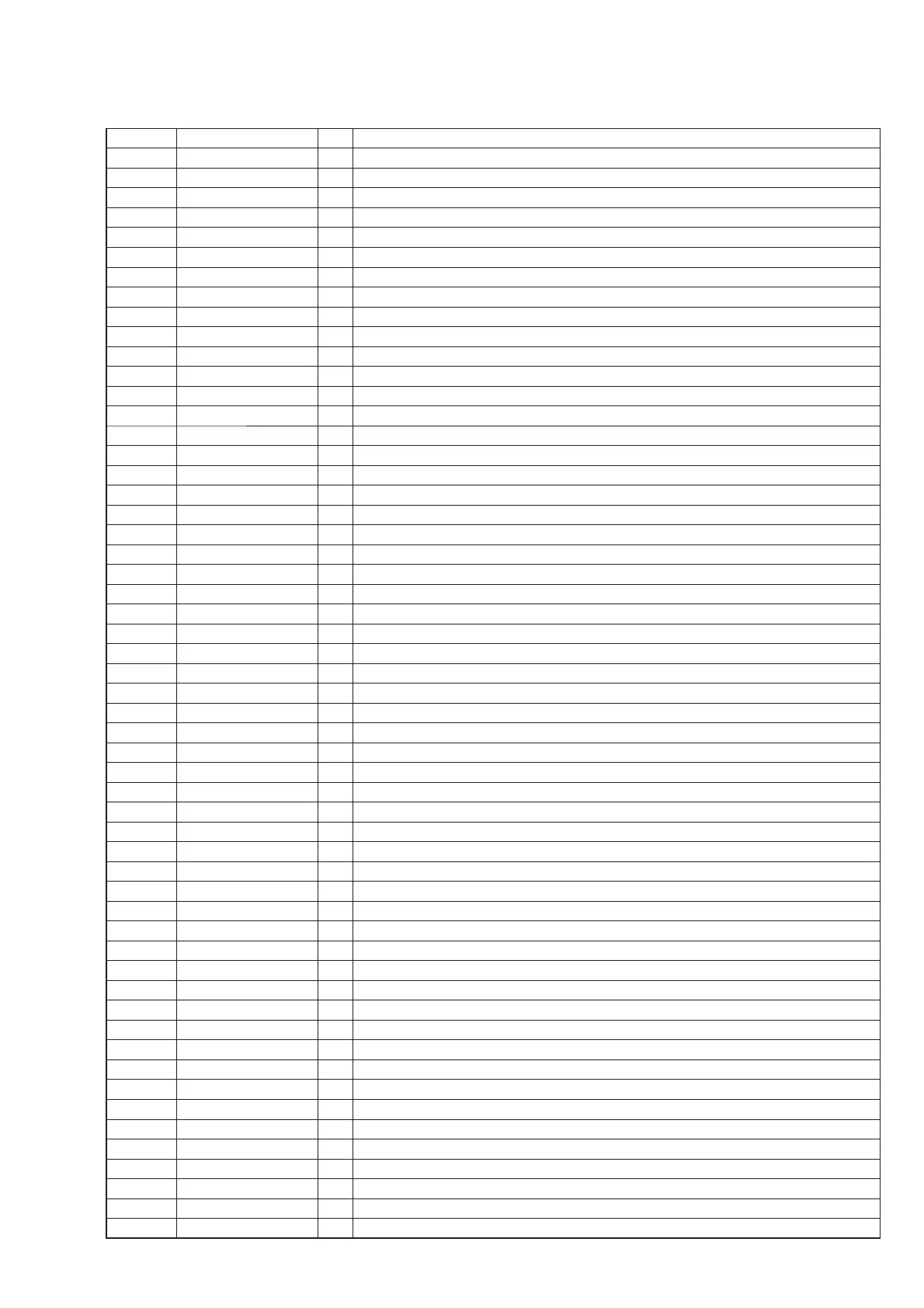
Pin No. Pin Name I/O Description
1 /RESET I Reset signal input from the system control IC (L: reset)
2 DI I Ready to send signal input from the system control IC
3, 4 NO USE O Not used. (Open)
5 G-3 I Function select signal input (Fixed at H in this set)
6 DVCC — Power supply pin (+3.2 V)
7 to 9 NO USE O Not used. (Open)
10 DVSS — Ground
11 DVCC — Connect to RVOUT1 in this set
12 RVOUT1 O External capacitor connection terminal
13, 14 RVIN I Reference voltage (+3.2 V) input
15 RVOUT2 O External capacitor connection terminal
16 DVCC — Connect to RVOUT2 in this set
17 DVSS — Ground
18 to 25 D0 to D7 I/O Two-way data bus input/output with the S-RAM IC
26 DVSS — Ground
27 DVCC — Power supply pin (+3.2 V)
28 to 35 D8 to D15 I/O Two-way data bus input/output with the S-RAM IC
36 A0 O Address signal output (Not used in this set)
37 to 43 A1 to A7 O Address signal output for the S-RAM IC
44 DVSS — Ground
45 DVCC — Power supply pin (+3.2 V)
46 to 54 A8 to A16 O Address signal output for the S-RAM IC
55 to 58 BUS0 to BUS3 O Serial data output for the CD-MP3 processor IC
59 /BUCK O Serial data transfer clock signal output for the CD-MP3 processor IC
60 /CCE O Chip enable signal output for the CD-MP3 processor IC
61 NO USE O Not used. (Open)
62 DVSS — Ground
63 DVCC — Power supply pin (+3.2 V)
64 RD O Read enable signal output for the S-RAM
65 WR O Write enable signal output for the S-RAM
66 SRLLB O Lower-byte control signal output for the S-RAM
67 SRLUB O Upper-byte control signal output for the S-RAM
68 NO USE O Not used. (Open)
69 BOOT I Boot mode select signal input (L: boot mode)
70 CS2 O Chip select signal output for the S-RAM
71 LRCK O L/R sampling clock signal output for the CD-MP3 processor IC
72 AM1 I Function mode select signal input (Fixed at H in this set)
73 X2 O System clock signal output (9 MHz)
74 DVSS — Ground
75 X1 I System clock signal input (9 MHz)
76 DVCC — Power supply pin (+3.2 V)
77 USBOC I USB over current detect signal input
78 USBPON O USB VBUS power ON/OFF control signal output (H: power ON)
79 D+ I/O Two-way data (positive) bus input/output with the USB connector
80 D- I/O Two-way data (negative) bus input/output with the USB connector
81 AM0 I Function mode select signal input (Fixed at H in this set)
82 NO USE O Not used. (Open)
83 DVSS — Ground
84 DO O Clear to send signal output for the system control IC
85 DATA I Audio data input from the CD-MP3 processor IC
86 CLOCK I Audio data transfer clock signal input from the CD-MP3 processor IC
87 TXD1 O Serial data output for the system control IC
88 RXD1 I Serial data input from the system control IC
89 NO USE O Not used. (Open)
90 SDA I/O Two-way EEPROM I2C data bus input/output (Not used in this set)




 To Next Page