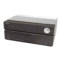
HCD-DJ2i
4
1. SERVICE NOTES .................................................. 5
2. GENERAL
Guide to parts and controls ............................................. 6
3. DISASSEMBLY
3-1. Panel (Bottom) ................................................................ 13
3-2. REGULATOR Board ...................................................... 13
3-3. MAIN AUDIO Board ..................................................... 14
3-4. MAIN DIGITAL Board .................................................. 14
3-5. Panel (Loading) ............................................................... 15
3-6. Bracket (CDM) ............................................................... 15
3-7. USB Board ...................................................................... 16
3-8. IR Board, MASTER VOL Board .................................... 16
3-9. EQ Board, CUE VOL Board ........................................... 17
3-10. DISPLAY Board, CROSS FADER Board ...................... 17
3-11. ESC Top Assy ................................................................. 18
3-12. CD Mechanism Block ..................................................... 18
3-13. Tray ................................................................................. 19
3-14. Belt, Base Unit ................................................................ 19
3-15. OP Base Assy .................................................................. 20
3-16. Optical Pick-up, BD93 Board ......................................... 20
4. TEST MODE ............................................................ 21
5. ELECTRICAL ADJUSTMENTS ........................ 25
6. DIAGRAMS
6-1. Block Diagram –CD Section– ........................................ 28
6-2. Block Diagram –Audio Section– .................................... 29
6-3. Block Diagram –Digital Section– ................................... 30
6-4. Block Diagram –Display/power Section– ...................... 31
TABLE OF CONTENTS
6-5. Printed Wiring Boards –CD Section– ............................. 33
6-6. Schematic Diagram –CD Section (1/2)– ........................ 34
6-7. Schematic Diagram –CD Section (2/2)– ........................ 35
6-8. Printed Wiring Boards –Main Digital Section– .............. 36
6-9. Schematic Diagram –Main Digital Section (1/2)– ......... 37
6-10. Schematic Diagram –Main Digital Section (2/2)– ......... 38
6-11. Printed Wiring Boards –Main Audio Section– ............... 39
6-12. Schematic Diagram –Audio Section (1/2)– .................... 40
6-13. Schematic Diagram –Audio Section (2/2)– .................... 41
6-14. Printed Wiring Boards –REGULATOR Section– ........... 42
6-15. Schematic Diagram –REGULATOR Section– ............... 43
6-16. Printed Wiring Boards –IPOD Section– ......................... 44
6-17. Schematic Diagram –IPOD Section– ............................. 45
6-18. Printed Wiring Board –USB Section– ............................ 46
6-19. Schematic Diagram –USB Section– ............................... 47
6-20. Printed Wiring Boards –Side A Section– ........................ 48
6-21. Schematic Diagram –Side A Section– ............................ 49
6-22. Printed Wiring Boards –Side B Section– ........................ 50
6-23. Schematic Diagram –Side B Section– ............................ 51
6-24. Printed Wiring Boards –Display Section– ...................... 52
6-25. Schematic Diagram –Display Section– .......................... 53
6-26. Schematic Diagram –Master VOL Section– ................... 54
6-27. Printed Wiring Boards –Master VOL Section– .............. 55
7. EXPLODED VIEWS
7-1. Panel Bottm Section ........................................................ 67
7-2. Panel Section-1 ............................................................... 68
7-3. Panel Section-2 ............................................................... 69
7-4. ESC Top Section ............................................................. 70
7-5. CD Mechanism Section .................................................. 71
8. ELECTRICAL PARTS LIST .............................. 72
 Loading...