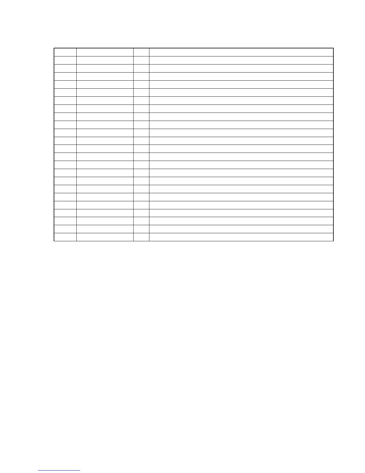
45
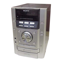
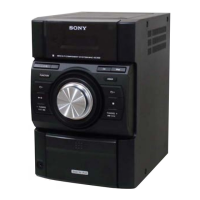
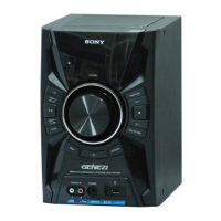
HCD-EC70
Pin No. Pin Name I/O Description
49 P74/SDA/SC2 I Data transfer request signal input from the MP3 decoder
50 P75/SCL/SO2 I Acknowledge signal input from the MP3 decoder
51 MD2 I Input pin for selecting operation mode (Connected to ground)
52 MD1 I Input pin for selecting operation mode (Connected to +3.3V)
53 MD0 I Input pin for selecting operation mode (Connected to +3.3V)
54 RSTX I System reset signal input terminal
55 V0/P80 O Tuner chip enable signal output to the tuner
56 V1/P81 O Clock signal output to the tuner
57 V2/P82 O Data output to the tuner
58 V3 I Reference power terminal of LCD controller/driver
59, 60 COM0, COM1 O Common signal output to the LCD
61, 62 P83/COM2, P84/COM3 O Common signal output to the LCD
63, 64 SEG0, SEG1 O Segment signal output to the LCD
65 VCC — Power supply terminal (+3.3V)
66 VSS — Ground terminal
67 to 84 SEG2 to SEG19 O Segment signal output to the LCD
85 to 89 SEG20/P10 to SEG24/P14 O Segment signal output to the LCD
90 VCC — Power supply terminal (+3.3V)
91 VSS — Ground terminal
92 X1 I Resonator input terminal (4.19MHz)
93 X0 O Resonator output terminal (4.19MHz)
94 to 96 SEG25/P15 to SEG27/P17 O Segment signal output to the LCD
97 to 100 SEG28/P20 to SEG31/P23 O Segment signal output to the LCD