1717
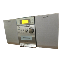
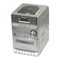
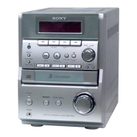
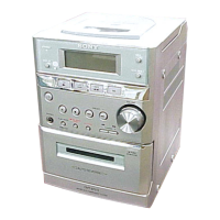
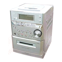
HCD-EP303
Note on Schematic Diagram:
• All capacitors are in µF unless otherwise noted. p: pF.
50 WV or less are not indicated except for electrolytics
and tantalums.
• All resistors are in Ω and
1
/
4
W or less unless otherwise
specified.
• 2 : nonflammable resistor.
• C : panel designation.
Note on Printed Wiring Board:
• W : indicates side identified with part number.
• : Pattern from the side which enables seeing.
(The other layers' patterns are not indicated.)
• Indication of transistor
• A : B+ Line.
• H : adjustment for repair.
•Voltages are taken with a VOM (Input impedance 10 MΩ).
Voltage variations may be noted due to normal produc-
tion tolerances.
•Waveforms are taken with a oscilloscope.
Voltage variations may be noted due to normal produc-
tion tolerances.
no mark : FM
<>: CD (STOP)
• Circled numbers refer to waveforms.
• Signal path.
F : FM
f : AM
E : PB (TAPE)
a : REC (TAPE)
J : CD PLAY
•Abbreviation
E51 : Chilean and Peruvian model.
MY : Malaysia model.
SP : Singapore model.
AR : Argentine model.
MX : Mexican model.
AUS: Australian model.
Note:
The components identi-
fied by mark 0 or dotted
line with mark 0 are criti-
cal for safety.
Replace only with part
number specified.
Note:
Les composants identifiés par
une marque 0 sont critiques
pour la sécurité.
Ne les remplacer que par une
piéce portant le numéro
spécifié.
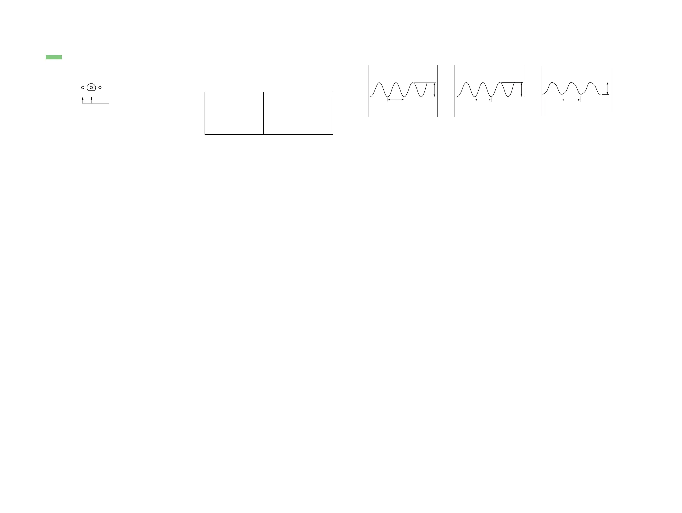
• WAVEFORMS
– MAIN Board – – CASSETTE Board – – DISPLAY Board –
1 IC102 ws (XOUT)
3.4 Vp-p
139 ns
1 V/DIV, 40 ns/DIV
2 Q705 (Collector)
(RECORD mode)
2 V/DIV, 4
µ
s/DIV
3 IC601 tl (X2)
1 V/DIV, 100 ns/DIV
6.0 Vp-p
12.4
µ
s
5.2 Vp-p
167 ns
B
These are omitted.
CE
 Loading...