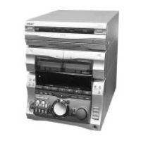
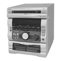
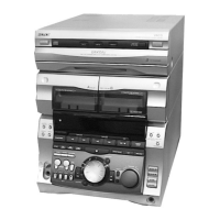
HCD-GRX20/RXD3
1919
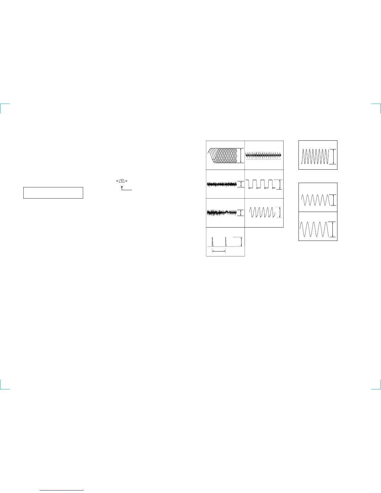
1
IC701 #£ (PLAY MODE)
2
IC701 2 (FEI)
(PLAY MODE)
3
IC701 $¶ (TEI)
(PLAY MODE)
4
IC703 @¶ (MDP)
5
IC702 $ª (B) GFS
7
IC702 &¡ (XTAO)
Approx. 1.0Vp-p
Approx. 0.1Vp-p
Approx. 0.1Vp-p
2.4Vp-p
0.1µsec/div
0.1V/div
7.7 µsec
5.7Vp-p
4.2336MHz
16.9344MHz
5.6Vp-p
(PLAY MODE)
8
IC601 $º (X' TAL)
4.8Vp-p
10MHz
7.2MHz
3.6Vp-p
9
IC103 @™ (X OUT)
90.790kHz
52Vp-p
!º
L251 7
(PLAY MODE)
(REC MODE)
6
IC702 %™ (A) C4M
— BD SECTION — — PANEL SECTION —
— MAIN SECTION —
• WAVEFORM
For schematic diagrams.
Note:
• All capacitors are in µF unless otherwise noted. pF: µµF
50 WV or less are not indicated except for electrolytics
and tantalums.
• All resistors are in Ω and
1
/
4
W or less unless otherwise
specified.
• % : indicates tolerance.
•
¢
: internal component.
• 2 : nonflammable resistor.
• 1 : fusible resistor.
• C : panel designation.
• U : B+ Line.
• V : B– Line.
• H : adjustment for repair.
• Voltages and waveforms are dc with respect to ground
under no-signal (detuned) conditions.
• Voltages are taken with a VOM (Input impedance 10 MΩ).
Voltage variations may be noted due to normal produc-
tion tolerances.
• Waveforms are taken with a oscilloscope.
• Circled numbers refer to waveforms.
• Signal path.
F : FM
f : AM
E : PB (DECK A)
d : PB (DECK B)
G : REC (DECK B)
J : CD
• Abbreviation
AUS : Australian model
SP : Singapore model
MX : Mexican model
AR : Argentina model
TW : Taiwan model
THIS NOTE IS COMMON FOR PRINTED WIRING
BOARDS AND SCHEMATIC DIAGRAMS.
(In addition to this necessary note is printed in each
block.)
The components identified by mark ! or dotted
line with mark ! are critical for safety.
Replace only with part number specified.
For printed wiring boards.
Note:
• X : parts extracted from the component side.
•
®
: Through hole.
•
¢
: internal component.
• b : Pattern from the side which enables seeing.
B
This is omitted.
CE
Q
• Indication of transistor.