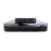
Do you have a question about the Sony HCD-HDX265 and is the answer not in the manual?
Details technical specifications of the product, including model names.
Specifies power output and harmonic distortion for US model audio.
Details amplifier section specifications for US models and other models.
Details DVD system, tuner, video sections, power requirements, and dimensions.
Highlights safety-related components and precautions for operation.
Describes methods to measure AC leakage current from exposed metal parts.
Explains self-diagnosis messages and troubleshooting steps for system malfunctions.
Details precautions for handling optical pick-up block and laser diode to prevent damage.
Explains characteristics and usage of unleaded solder and its mark.
Procedures to release tray lock and demo play lock functions.
Notes on EEPROM exchange and model part numbers for identification.
Explains symbols used in the manual and provides notes on disc formats and playback.
Details playable disc formats, limitations, region code, and playback operations.
Guides on how to identify the correct optical pick-up block for replacement.
Procedure to open the disc tray when the power switch is off.
Illustrates the service position for the main board during repair.
Details checks for harness settings during service to ensure proper connection.
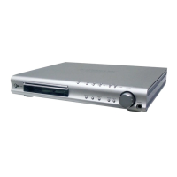
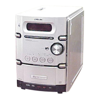
Identifies and describes the controls and indicators on the front panel.
Lists and describes all rear panel connection terminals and ports.
Explains the meaning of various indications shown on the front panel display.
Details the function of each button on the remote control for system operation.
Provides a step-by-step flow for disassembling the unit.
Step-by-step guide to removing the unit's outer case.
Instructions for safely removing the DIAT CON board.
Steps to remove the IO board, including cable disconnections.
Guide for taking apart the front panel assembly.
Procedure to remove the power board and its connectors.
Steps to disassemble the back panel block assembly.
Instructions for removing the DMPORT board.
Steps for safely removing the MAIN board.
Procedure to remove the MD cover.
Steps to disassemble the DVD mechanism deck.
Steps to disassemble the main tray assembly.
Procedure to remove the motor board.
Steps to disassemble the base unit.
Procedure for removing the optical pick-up block.
Precautions for gear installation and details on sub tray gears.
Steps to disassemble the lever assembly.
Procedure for disassembling the stocker section.
Precautions for installing cam (stocker) components.
Precautions for installing the stocker 3 gear.
Precautions for installing the rotary encoder (MD).
Precautions for assembling the BU1 gear.
Procedures for cold reset and panel test mode.
Details version test, key test, and disc tray lock procedures.
Guides for ship mode, AM step change, and product out modes.
Procedure for automatic acoustic field calibration test mode.
Procedures for demo play out and volume test modes.
Details DVD color system switching and protection identification modes.
Step-by-step guide for testing the DMPORT.
General description and procedure to enter DVD service mode.
Instructions for executing IOP measurement.
How to access and check the system's emergency history.
Explains error codes, parameters, and time of occurrence.
Procedures to clear laser hours and emergency history.
Steps to initialize setup data and return to the diagnosis menu.
Procedure to check firmware, RISC, DSP, and other version information.
Procedures for adjustments in the DVD section.
Procedure to check FM tuner tune level reception.
Block diagram showing RF servo and video signal paths.
Block diagram illustrating changer, HDMI, and DMPORT sections.
Block diagram detailing the audio processing path.
Block diagram illustrating the amplifier stages and power output.
Block diagram for panel display, controls, and power supply.
Explains symbols and notations used in schematics and PWB diagrams.
Identifies the location of major circuit boards within the unit.
Schematic diagram for the MAIN board, part 1 of 13.
Schematic diagram for the MAIN board, part 2 of 13.
Schematic diagram for the MAIN board, part 3 of 13.
Schematic diagram for the MAIN board, part 4 of 13.
Schematic diagram for the MAIN board, part 5 of 13.
Schematic diagram for the MAIN board, part 6 of 13.
Schematic diagram for the MAIN board, part 7 of 13.
Schematic diagram for the MAIN board, part 8 of 13.
Schematic diagram for the MAIN board, part 9 of 13.
Schematic diagram for the MAIN board, part 10 of 13.
Schematic diagram for the MAIN board, part 11 of 13.
Schematic diagram for the MAIN board, part 12 of 13.
Schematic diagram for the MAIN board, part 13 of 13.
Printed wiring board layout for the MAIN board, component side.
Printed wiring board layout for the MAIN board, conductor side.
Printed wiring board layouts for the SIRIPARA board.
Schematic diagram for the SIRIPARA board.
Printed wiring board layouts for the changer section components.
Schematic diagram for the changer section.
Printed wiring board layouts for the DMPORT board.
Schematic diagram for the DMPORT board.
Schematic diagram for the IO board, part 1 of 2.
Schematic diagram for the IO board, part 2 of 2.
Printed wiring board layout for the IO board.
Printed wiring board layout for the FL board.
Schematic diagram for the FL board, part 1 of 2.
Schematic diagram for the FL board, part 2 of 2.
Printed wiring board layouts for panel section components.
Schematic diagram for the panel section.
Schematic diagram for the POWER board, part 1 of 2.
Schematic diagram for the POWER board, part 2 of 2.
Printed wiring board layout for the POWER board.
Illustrates waveform examples for key signal points on the MAIN board.
Illustrates waveform examples for key signal points on the IO board.
Simplified block diagrams for key ICs on the MAIN board.
Block diagrams for CXD9843AR stream processor ICs.
Block diagram for the TC7WH157FK selector IC.
Block diagrams for CXD9883M power amplifier ICs.
Block diagrams for BH2210FV-E2 ICs on the SIRIPARA board.
IC block diagrams for Relay, DMPORT, and IO boards.
Block diagrams for BU2099FV and PD16315GB-3BS ICs on the FL board.
Block diagrams for STR-F6138/F6168 and STR-V153 ICs on the POWER board.
Block diagrams for SI-3010KM-TL ICs used in power supply.
Pinout description for the SYSTEM CONTROLLER IC501 on the MAIN board.
Continues pinout description for IC501, covering pins 44 to 96.
Final pinout description for IC501, covering pins 97 to 100.
Pinout description for IC1101 (RF AMP, SERVO DSP, MPEG DECODER).
Continues pinout description for IC1101, covering pins 49 to 130.
Continues pinout description for IC1101, covering pins 131 to 190.
Continues pinout description for IC1101, covering pins 191 to 241.
Continues pinout description for IC1101, covering pins 242 to 256.
Pinout description for IC1701 (HDMI TRANSMITTER).
Continues pinout description for IC1701, covering pins 65 to 80.
Exploded view of the unit's case, showing part numbers and assembly.
Exploded view of the front panel assembly, listing parts.
Exploded view of the main section, showing major assemblies and parts.
Exploded view of the DVD mechanism deck, part 1.
Exploded view of the DVD mechanism deck, part 2.
Exploded view of the DVD mechanism deck, part 3.
Exploded view of the base unit, including pick-up block and motors.
List of electrical parts for the DIAT CON board.
Parts list for EN and LED boards, including capacitors and LEDs.
Lists transistor and resistor parts.
Parts list for capacitors, connectors, diodes, ICs, and coils.
Lists more transistor and resistor parts.
Continues listing capacitor parts.
Continues listing capacitor parts.
Continues listing capacitor parts.
Parts list for connectors, diodes, ICs, and jack terminals.
Lists ICs, coils, transistors, and resistors.
Continues listing resistor parts.
Continues listing resistor parts.
Continues listing resistor parts.
Continues listing resistor parts.
Parts list for capacitors, connectors, diodes, ICs, coils, and transistors.
Lists parts for fuses, ICs, coils, transistors, and resistors.
Lists parts for resistors, terminals, switches, and capacitors.
Lists parts for ICs, resistors, speaker board, and switches.
Lists miscellaneous parts like tuners, cords, fuses, fans, and encoders.
Details changes to main, DMPORT, EN, LED, DIAT CON, SPEAKER, and PW-SW boards.
Compares former and new part numbers for key boards.
Revised schematic for the MAIN board, part 1 of 13.
Revised schematic for the MAIN board, part 2 of 13.
Revised schematic for the MAIN board, part 3 of 13.
Revised schematic for the MAIN board, part 4 of 13.
Revised schematic for the MAIN board, part 5 of 13.
Revised schematic for the MAIN board, part 6 of 13.
Revised schematic for the MAIN board, part 7 of 13.
Revised schematic for the MAIN board, part 8 of 13.
Revised schematic for the MAIN board, part 9 of 13.
Revised schematic for the MAIN board, part 10 of 13.
Revised schematic for the MAIN board, part 11 of 13.
Revised schematic for the MAIN board, part 12 of 13.
Revised schematic for the MAIN board, part 13 of 13.
Revised PWB layout for the MAIN board, component side.
Revised PWB layout for the MAIN board, conductor side.
Revised PWB layout for the DMPORT board.
Revised schematic diagram for the DMPORT board.
Revised PWB layouts for panel section components.
Revised schematic diagram for the panel section.
Parts list for DIAT CON, DMPORT, and EN boards.
Parts list for LED board, capacitors, connectors, LEDs, transistors, and resistors.
Continues listing capacitor parts.
Continues listing capacitor parts.
Parts list for diodes, ICs, coils, transistors, and resistors.
Continues listing resistor parts.
Continues listing resistor parts.
Continues listing resistor parts.
Continues listing resistor parts.
Continues listing resistor parts.
Continues listing resistor parts.
Parts list for capacitors, connectors, and terminals.
Lists manual versions, dates, and descriptions of revisions.